Continue to Site

Welcome to EDAboard.com

Welcome to our site! EDAboard.com is an international Electronics Discussion Forum focused on EDA software, circuits, schematics, books, theory, papers, asic, pld, 8051, DSP, Network, RF, Analog Design, PCB, Service Manuals... and a whole lot more! To participate you need to register. Registration is free. Click here to register now.

LDO: load resistance negligible?

Status
Not open for further replies.

tzg6sa

Member level 2
Joined
Jun 3, 2008
Messages
44
Helped
3
Reputation
6
Reaction score
3
Trophy points
1,288
Location
Hungary
Activity points
1,581
Hi All,

I have read the beginning of Ricon-Mora's PhD thesis, where I found the following statement by the AC analysis, what I do not understand.
"The output resistance of the load is commonly neglected because its value is considerably larger than Rx."
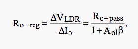
Where Rx = Ropass||'feedback divider'.
The pass transistor is a controlled current source, thus its output impedance is high. (At least few kohms) The feedback divider's resistance must be high to lower the quiescent current.
If I assume 1.8V output voltage and 6mA load current, then the load resistance is just 300ohm, which is not negligible at all. It would be negligible for a few uA load current.

Am I missing the obvious?
 

Hi tzg6sa,

Did you realize that the BJT normally is operated in common collector configuration (emitter follower) with a rather low output resistance?
 

The pass element is a common source pMOS. It is not said explicitly but it is treated in the analysis as a voltage controlled current source with a parallel output impedance Ropass.

How can be a common collector pass transistor feasible in an LDO? (low drop-out regulator) The gate-source voltage of the pass transistor should be lower than the drop-out voltage. Am I wrong?
 

No, of course, you are right if it`s a common source PMOS.
By calculating the effective output impedance, however, not only the "feedback divider" has to be taken into consideration, but instead the whole feedback circuit (including the high gain error amplifier) and it's influence on the pass transistor.
From feedback theory it is known that this kind of feedback lowers the output resistance considerably. This effect leads to a sufficient small output impedance of the control loop which enables the whole circuit to work nearly as a voltage source, which only very little is influenced by load changes.
 

    tzg6sa

    Points: 2
    Helpful Answer Positive Rating
tzg6sa said:
... The pass transistor is a controlled current source, thus its output impedance is high. (At least few kohms)
Am I missing the obvious?
I'd think so: The pass transistor's output resistance is rather low (even if it isn't an emitter or source follower, but a common emitter/source pass transistor) because of the fact that it is embedded into the feedback loop of the amplifier. As with any amplified system, its "natural" output resistance is still divided by the loop gain of the amplifier, s. equ. 1.3 of Rincón-Mora's thesis on p. 8 (PDF p. 28 ):
31_1265889259.gif


With a common source pass transistor, nearly the full primary power supply voltage can be used to control its gate voltage.
 

    tzg6sa

    Points: 2
    Helpful Answer Positive Rating
I understand that in close loop, the impedance look from output node into LDO, the impedance is small.

However, during open-loop ac analysis, isn't the load resistance should be considered, and the load resistance is much smaller than the Ro_pass?
 

duet12 said:
... during open-loop ac analysis, isn't the load resistance should be considered, and the load resistance is much smaller than the Ro_pass?
Why would you like to run the ac analysis in open-loop? This wouldn't give you realistic results! Closed-loop is the real application, and if you want to know the actual behaviour of the circuit vs. frequency, you should of course run the analysis on the real circuit, i.e. in closed-loop!
 

Thanks for your reply.

The open-loop analysis here refers to
1. break the loop by inserting the a super big inductor between feedback node and the input of diff pair.
2. Add a AC input to the input of diff pair with a super big capacitor.

By doing that, the loop is break and ac simulation is performed. From simulation, the output pole varies significantly with the way the current load is implemented.

If directly using an ideal current source, the pole would be determined by the Ro_pass
If using a resistor to draw current, the pole would be significantly affected by the resistor.

So the confusion here is which implementation of current load is more realistic.

BTW, when we are determining the location of output pole, are we not supposed to consider the effect of close-loop?
 

duet12 said:
The open-loop analysis here refers to
1. break the loop by inserting the a super big inductor between feedback node and the input of diff pair.
2. Add a AC input to the input of diff pair with a super big capacitor.

By doing that, the loop is break and ac simulation is performed. From simulation, the output pole varies significantly with the way the current load is implemented.
Thank you for this summary, Duet,
this all is well-known stuff, and I think the open-loop simulation is quite ok for a first check in order to find the original poles and zeroes, open-loop gain, bandwidth a.s.o. The real application, however, is always running in closed-loop, and this changes all the a.m. properties quite a lot. If you really want to know the actual properties of your application circuit, you better run your analysis on the circuit as it is configured, i.e. in its closed-loop configuration.

duet12 said:
If directly using an ideal current source, the pole would be determined by the Ro_pass. If using a resistor to draw current, the pole would be significantly affected by the resistor. So the confusion here is which implementation of current load is more realistic.
No confusion: Again use the simulation configuration of the real application, whatever it is - constant current, or resistive, or resistive+capacitive. If you don't know before, analyze all possible configurations.

duet12 said:
BTW, when we are determining the location of output pole, are we not supposed to consider the effect of close-loop?
Now you got it right! And only in this way you get to know the correct output impedance.
 

Quote ERIKL:

......this all is well-known stuff, and I think the open-loop simulation is quite ok for a first check in order to find the original poles and zeroes, open-loop gain, bandwidth a.s.o. The real application, however, is always running in closed-loop, and this changes all the a.m. properties quite a lot. If you really want to know the actual properties of your application circuit, you better run your analysis on the circuit as it is configured, i.e. in its closed-loop configuration.

Hi ERIK,
just a few comments. An LDO is a circuit to be designed according to control theory laws.
During open loop analysis you do NOT find "original poles and zeros" for closed-loop operation.
The only purpose of the open-loop analysis is to see the loop gain and its phase in order to verify stability properties after closing the loop. Doing an ac analysis only for the closed loop not always gives the right information about stability properties.
 

Hi LvW,
LvW said:
Hi ERIK,
An LDO is a circuit to be designed according to control theory laws.
Did you think of something like "consider, follow, observe, adhere to"?

LvW said:
During open loop analysis you do NOT find "original poles and zeros" for closed-loop operation.
Of course. I should have said: "During open-loop analysis you find "original poles and zeros" for open-loop operation."

LvW said:
The only purpose of the open-loop analysis is to see the loop gain and its phase in order to verify stability properties after closing the loop. Doing an ac analysis only for the closed loop not always gives the right information about stability properties.
Fully agree!
 

Status
Not open for further replies.

Part and Inventory Search

Welcome to EDABoard.com

Sponsor

Back
Top