NiedeLu
Junior Member level 3
Hi experts,
as I'm not very familiar with layout and I intend to do my first one, I have some questions:
For my circuitry I need some matched serial stacked PMOS transistors with the bulk connected to the same node (VDD). During the design phase I used 4 terminal devices of the PDK.
This is how one of this devices looks like (P-cell) -> P-Cell.PNG
(no bulk connection included)
For matching purpose I used a common centroid layout at each stage of the serial stack. I wanted to share the same NWELL with all transistors.
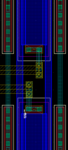
1. If I draw a NWELL over the complete stacked transistor block I get some shorts from diffusion to VDD (NWELL). But not for all diffusions. Please have a look at the attachment -> Stack2.PNG + Stack.PNG.
Can anyone explain why I get this shorts? Or is it just a tool issue?
2. Is the bulk connection done in a right way? I used NTAPS over the whole NWELL.
Kindly asking for your help.
BR
Lukas
Edit: shorts can be seen as yellow crossed rectangulars
as I'm not very familiar with layout and I intend to do my first one, I have some questions:
For my circuitry I need some matched serial stacked PMOS transistors with the bulk connected to the same node (VDD). During the design phase I used 4 terminal devices of the PDK.
This is how one of this devices looks like (P-cell) -> P-Cell.PNG
(no bulk connection included)
For matching purpose I used a common centroid layout at each stage of the serial stack. I wanted to share the same NWELL with all transistors.
1. If I draw a NWELL over the complete stacked transistor block I get some shorts from diffusion to VDD (NWELL). But not for all diffusions. Please have a look at the attachment -> Stack2.PNG + Stack.PNG.
Can anyone explain why I get this shorts? Or is it just a tool issue?
2. Is the bulk connection done in a right way? I used NTAPS over the whole NWELL.
Kindly asking for your help.
BR
Lukas
Edit: shorts can be seen as yellow crossed rectangulars