maheshkuruganti
Advanced Member level 4
Layout Help
Hey,
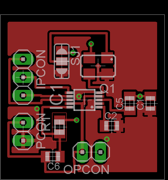
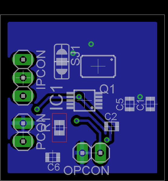
I layed out a Double Sided SMD PCB for my AD9833.The Top layer is a VDD pour and bottom layer is a VCC Pour.I don't know if this layout is a good plan so I want to know if someone could tell me how to improve it.
P.S: This has to hand soldered by pro(not me) so any ideas regarding increasing Solderability are also welcome.Thanks.
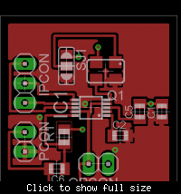
Top view
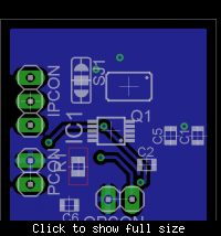
Bottom View
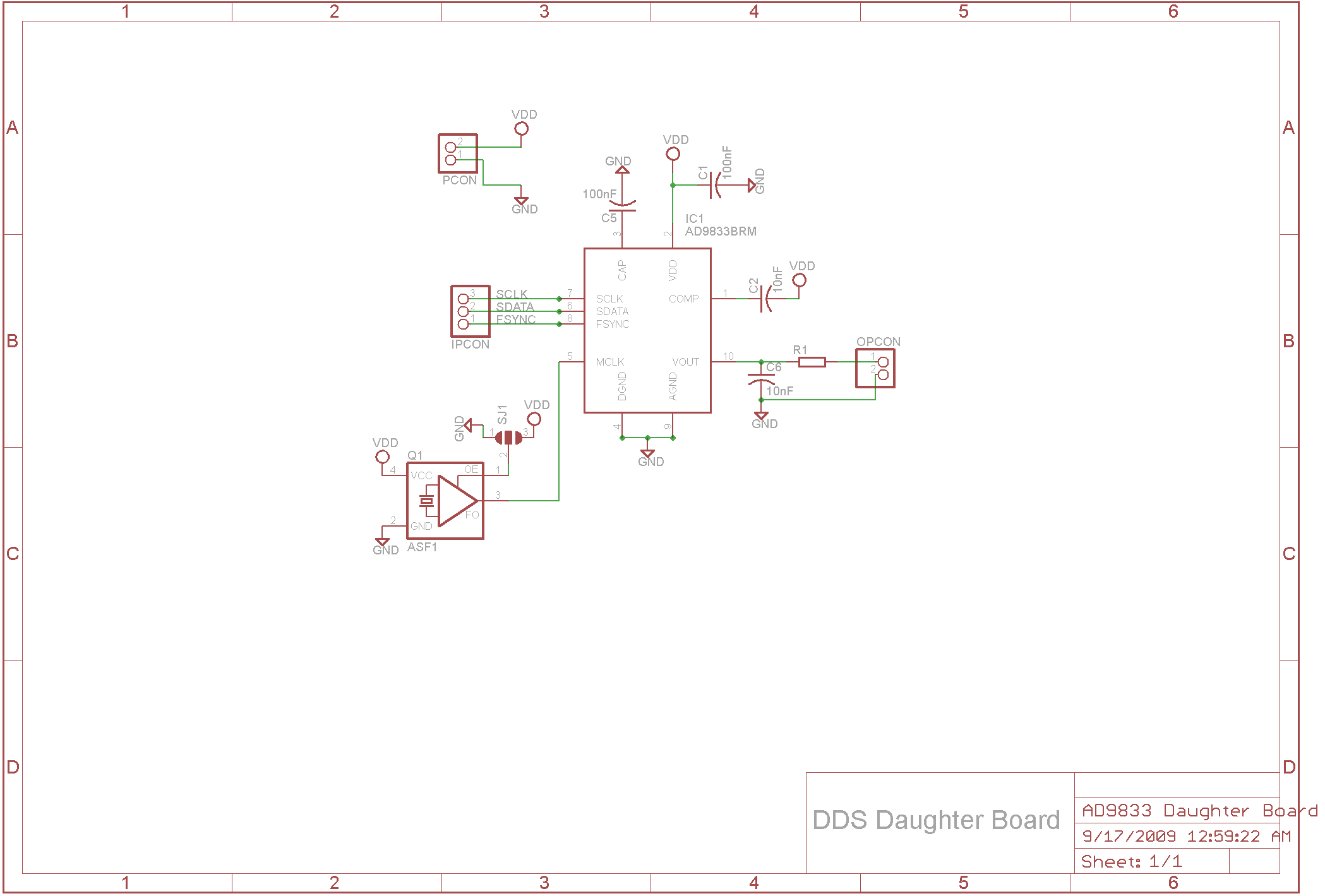
Schematic View
Hey,
I layed out a Double Sided SMD PCB for my AD9833.The Top layer is a VDD pour and bottom layer is a VCC Pour.I don't know if this layout is a good plan so I want to know if someone could tell me how to improve it.
P.S: This has to hand soldered by pro(not me) so any ideas regarding increasing Solderability are also welcome.Thanks.
Top view
Bottom View
Schematic View