skysky
Newbie level 6
latchup
discription:
the simulation result of current of the IC is less than 10uA,
but the test result is more than 170mA.
When measuring , the current of the IC first rise to 10mA slowly, then reach 170mA quickly.
So, I think that latch-up happens somewhere. The question is that which device induce latch-up?
The doubtful schematic is shown in the figure.
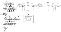
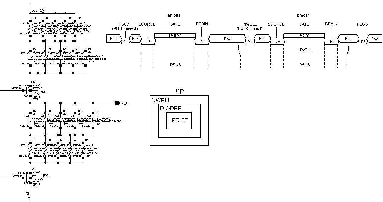
 4> are in a separate n-well (separate from <D5