Continue to Site

Welcome to EDAboard.com

Welcome to our site! EDAboard.com is an international Electronics Discussion Forum focused on EDA software, circuits, schematics, books, theory, papers, asic, pld, 8051, DSP, Network, RF, Analog Design, PCB, Service Manuals... and a whole lot more! To participate you need to register. Registration is free. Click here to register now.

keep-out area around footprint

Status
Not open for further replies.

Kick

Full Member level 6
Joined
Sep 27, 2010
Messages
344
Helped
16
Reputation
32
Reaction score
15
Trophy points
1,298
Location
India,Bangalore
Activity points
3,170
hiii all,
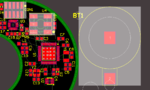
I have a problem in Altium PCB doc. In my project some footprints designed by me only. Problem is a transparent keep-out area is visible (while clicking above that footprint) around that footprints,because of that I can't place components near to that footprint,but I can route in that area. How can I solve this problem?? Can I edit that area?
 

what type of keepout u desired to mean? (whether package or route)
 

you can see in this attachment.
 

Attachments

  • image.png
    image.png
    81.9 KB · Views: 225

From my understanding you speak about the place bound top of footprint. Due to that you suffer while placing the component. Edit (reduce) that place bound area as you want. And try that.
 

It can't change directly on board. For that you modify in footprint at first. Then update in board . In (allegro PCB editor)place option drop-down has manually option in that select package symbol. From that update it.
 

For footprint of each component have any layer???????????
 

you can see in this attachment.

The gray transparent box seen in the screenshot only identifies the perimeter in which all of the primitives of the selected component are contained within. That includes the pads, 3D body, silkscreen, assembly drawing info, etc. for the selected part. Everything except the reference designator. The box is always rectangular and just assists you in identifying the overall "size" of the component that you have selected. If the part is not selected, this box will not be visible.

However, your electrical clearance and component clearance (assuming the component has a 3D body defined) are not calculated or determined from this box at all (except in the missing 3D-body case mentioned below). For your electrical/copper clearance, the clearance is defined in the 'Electrical > Clearance' design rule set and only applies to primitives on copper layers (pads, vias, polygons, keepouts, etc.) For the component clearance (physical body clearance), the clearance is based on the 'Placement > Component Clearance' design rule set and applies specifically to the clearance between 3D Body layer content. However, if you do not have any 3D body model information (simple or step) defined in the component footprint (typically on layer 13 & 16), the component clearance will be calculated from the gray transparent box shown in your screenshot. Do you have 3D bodies defined in the problematic footprints you created? If you add some basic 3D body information to the footprint, you can maximize the component density on the board and prevent those DRC component clearance errors. There are several other clearance rules (like silk to silk, silk to board edge, etc.) but the component clearance rule is likely the problem in your case.

Good luck.
 
  • Like
Reactions: Kick

    Kick

    Points: 2
    Helpful Answer Positive Rating
thanks for your detailed explanation.I made the rule changes in 'Placement > Component Clearance' option,now the problem is solved.
 

Status
Not open for further replies.

Part and Inventory Search

Welcome to EDABoard.com

Sponsor

Back
Top