Continue to Site

Welcome to EDAboard.com

Welcome to our site! EDAboard.com is an international Electronics Discussion Forum focused on EDA software, circuits, schematics, books, theory, papers, asic, pld, 8051, DSP, Network, RF, Analog Design, PCB, Service Manuals... and a whole lot more! To participate you need to register. Registration is free. Click here to register now.

IR2110 Lo and Ho not switching

Status
Not open for further replies.

hornbrd

Newbie level 3
Joined
Nov 19, 2010
Messages
3
Helped
0
Reputation
0
Reaction score
0
Trophy points
1,281
Activity points
1,314
Hi everyone, I'm new to this site and new to using forums in general.

I have 2 IR2110 Ic's that run 4 FGA25N120 IGBT trench gates. I am supplying the Lin and Hin with a PWM signal from a LM555. The output on the 555 seems to be switching ok, but when checking the HO and LO output is where I have my problems. Ho stays closed on Q1 and Q3 with around 7V and LO has is open on Q2 and Q4. I'll try to add my drawing of what is going on, but like i said i'm new to this.
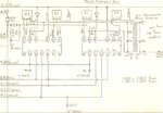
Power.jpg


I have been working with this circuit and other parts of it for awhile now, and in the beginning I think everything worked, but here lately I have not been able to get the IR2110 to switch. Any help would be greatly appreciated.
 

The VDD and VSS connection is incorrect. Consult the datasheet. VSS must be connected to V- and VDD to a 12 to 15 V positive supply.
 

I have about 12 V going into Vss. If I run the 100nf cap between Vss and Vdd then do i just ground Vdd, or does it need it's own power supply?
 

Sorry about the picture. The Vss and Vdd are not drawn in the correct place, they should be reversed. I tried hooking up +12 V to Vdd and ran the cap between it and Vss and grounded Vss. I'm still not getting any type of switching. Ho is staying high at around 8 V and Lo is nothing. Do have any other suggestions? This is for a project that i'm working on for school and the deadline is coming very quickly and I would like to have something working.

Thanks guys
 

Hi.. i am working on the same stuff now..
The following are my findings

1- the VDD, VCC and the DC bus should use same ground
2- the voltage VDD should have the same amplitude of your 555 timer output
3- use bootstrap capacitors in the range 1uF to 4 uF in kHz switching ranges
4- check all supply are connected with grounds as i mentioned
5- use same ground for 555 and ir 2110 circuit .. as far as possible try to derive the various auxillary voltage supplies needed from a single source

try it .. and please don't forget to put your comment back ... wish you success
 
The VDD and VSS connection is incorrect. Consult the datasheet. VSS must be connected to V- and VDD to a 12 to 15 V positive supply.

Hi fvm. in one of the post you make you mention that vdd is connected to 5v but why is it 12 to 15 v here?
 

Why are you using IGBT for 24 vdc primary? You can do better with MOSFET's at this voltage. You will get lower drain to source voltage drop with MOSFET's. With only 24v you need to strive for minimum voltage drops. Don't put a diode in series with your high current line. A parallel placement (cathode to Vin+, anode to Vin-) will protect reverse polarity by blowing fuse.

For bootstrap cap, you should have a lower value, good high frequency cap in parallel with the 10 uF. Like 0.1 uF ceramic.

The Vb to Vss voltage is running the high side gate turn on. Should be 12v to 15v to get good drive for gate.

Vs should be independent connection directly to highside FET source. Same for Com going directly to lowside FET source. This avoids any high current voltage drop in FET line from eating up gate drive voltage and creating unwanted feedback. Driver supplies should be independent regulated 12v to 15v supplies.

You should measure the leakage inductance on transformer to understand a reasonable filter arrangement for output. 35 uF seems a bit high in value and is going to give you a high idle current.

Transformer of this type of inverter arrangement are usually designed with a bit higher leakage inductance then a normal power transformer. This gives some inductance for the output cap to work against for the first output filter.
 
Last edited:
  • Like
Reactions: Rinson

    Rinson

    Points: 2
    Helpful Answer Positive Rating
hi ... you have mentioned about using a .1uF ceramic capacitor in parallel with 10uF electrolytic capacitor for bootstrap operation .. is it necessary ? what is the significance of the .1uF ceramic capacitor ? What does it do ?
 

MOSFET gate drive is short high current pulses during transitions. You want to be able to supply the high current pulse. This requires a good high frequency cap that gives up its charge quickly. A 0.1 uF will do this better then a 10 uF electrolytic.
 

    V

    Points: 2
    Helpful Answer Positive Rating
MOSFET gate drive is short high current pulses during transitions. You want to be able to supply the high current pulse. This requires a good high frequency cap that gives up its charge quickly. A 0.1 uF will do this better then a 10 uF electrolytic.

k... i am using 3.3 uF electrolytic capacitor for bootstrap operation as well as the capacitor for lower bridge capacitor .. don't dell me that it will not work ? :(
 

i think the problem is not in capasitor. If u using capasitor bootsrap too small value, the MOSFET high side still switching. but if the input logic high too long and the capacity of the capasitor have empty, the output switching is low...
 
. If u using capasitor bootsrap too small value, the MOSFET high side still switching. but if the input logic high too long and the capacity of the capasitor have empty, the output switching is low...

That is not how driving a MOSFET for a switcher works. Assuming input gate charge is 200 nC and switcher running at 25 kHz with a 200 nsec switching transistion. The gate drive current impulse for the 200 nsec will be 500 mA. A 0.1 uF cap will droop 1 volt of the 12v to 15v bootstrap precharge. If electrolytic has ESR of 1 ohm it will have the equivalent average droop, no matter how large capacitance value.
 

HI, can you explain it more clearer please it seems i dont understand what RC in FLA was saying.
 
Last edited:

For MOSFET gate drive, it's the transition that draws current, not how long the logic is high or low. Because you need a short high current spike from the driver during the logic transition, you need a capacitor with good high frequency performance, able to take charge and give up charge quickly.

In above example with 200 nsec transition, the effective series resistance of cap needs to be measured at a test frequency of 1/(2 x 200 nsec) or 2.5 MHz, not the 25 kHz switcher frequency.

Most electrolytic caps do not have good ESR at such a high frequency.
 
Last edited:

Status
Not open for further replies.

Similar threads

Part and Inventory Search

Welcome to EDABoard.com

Sponsor

Back
Top