Continue to Site

Welcome to EDAboard.com

Welcome to our site! EDAboard.com is an international Electronics Discussion Forum focused on EDA software, circuits, schematics, books, theory, papers, asic, pld, 8051, DSP, Network, RF, Analog Design, PCB, Service Manuals... and a whole lot more! To participate you need to register. Registration is free. Click here to register now.

Impedance controlled trace

Status
Not open for further replies.

pkaras

Junior Member level 1
Joined
Aug 5, 2010
Messages
16
Helped
0
Reputation
0
Reaction score
0
Trophy points
1,281
Activity points
1,415
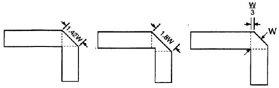
I am trying to draw an impedance (50 Ohm) controlled trace. I am going to use coplanar waveguide. I have read that chamfering is the recommended method for bends.
I have calculated that I need to use 40 mil wide trace and I need to leave gaps of 8 mil. I have also calculated M (percentage chamfer), which supposed to be ~78 (conductor height is 60 mil).

I would like to know if I did everything correctly. I am using chamfering technique for the first time and it seems a bit unusual to see the bend so thin.

I attach two images where one shows regular 40 mil wide trace and another shows trace that is chamfered. Does it look like it supposed to be?
Btw, ground plane is not displayed.


If the trace is part of a coplanar waveguide, you would look at the ground shape as well.

Firstly, you should mention frequency range and intended impedance accuracy respectively VSWR. Where did you get the 78% chamfer percentage. It seems to me as an overcorrection.
 

There are few equations that allow to calculate the 90-deg chamfer line.
Those equations are valid only for W/h > 0.25, where W is width of the line, and h is the height of the substrate.


If the trace is part of a coplanar waveguide, you would look at the ground shape as well.
Yes it is. Ground is just a solid plane on top layer and bottom layer (I will be using 2 layer board).

mW24v.PNG

Firstly, you should mention frequency range and intended impedance accuracy respectively VSWR.
~2.4Ghz. With regards to impedance accuracy, I am aiming for the best I can get in my situation (2 layer board, trace length - 16 mm)

Where did you get the 78% chamfer percentage.

iv7tc.PNG

It seems to me as an overcorrection.
It does not look right for me as well.
 
Last edited by a moderator:

The chamfer does a compensation of the corner's shunt capacitance by adding series inductance. Your microstrip calculation for the chamfer isn't accurate for the CPW (or grounded CPW?) case, because that capacitances are different. The most accurate solution would be to test your layout with an EM solver.
 
  • Like
Reactions: pkaras

    pkaras

    Points: 2
    Helpful Answer Positive Rating
volker@muehlhaus, I see. Can you recommend any software that I could use as EM solver? Is it a difficult procedure to test a layout?

I have used AppCAD to verify that 40 mil (width) and 8 mil (gap) numbers are correct. Are those calculations relevant only for the straight trace? If I decide to go with a regular trace (2nd picture in my first post) that has 45 degree bends, do I still need to use EM solver to get accurate calculations?

Btw, I use CPW with groundplane.
 

CPW with groundplane has a larger part of the capacitance located in the lateral ground, compensation of bends is less important than for microstrip. Secondly, if you worry about the chamfer calculation, why don't you use arcs instead of miters?
 

Arcs should have a radius of at least 3x the route width. I have 2 bends, so I get 2 x 3 x 40mil = 240mil. I don't have that much space.
 

Good results can be obtained using a radius of just 2x line width.
 

Status
Not open for further replies.

Similar threads

Part and Inventory Search

Welcome to EDABoard.com

Sponsor

Back
Top