Continue to Site

Welcome to EDAboard.com

Welcome to our site! EDAboard.com is an international Electronics Discussion Forum focused on EDA software, circuits, schematics, books, theory, papers, asic, pld, 8051, DSP, Network, RF, Analog Design, PCB, Service Manuals... and a whole lot more! To participate you need to register. Registration is free. Click here to register now.

idea for dual edge Linear_feedback_shift_register

Status
Not open for further replies.

ABO_ATHAB

Junior Member level 1
Joined
Dec 19, 2011
Messages
16
Helped
0
Reputation
0
Reaction score
0
Trophy points
1,281
Visit site
Activity points
1,403

Hi! Dual edge "thingy A" so therefor context is dual edge "thingy B"? That makes perfect sense!

Or in other words ... why the hell do you think an implementation of a dual edge counter has anything to do with a dual edge lfsr? Other than generic bag of tricks when doing ddr stuff...

The general idea is, did you actually read the thread? FvM's last post pretty much sums it up. So how are you planning to transpose that trick to the lfsr problem domain? What's that you say? eehhrrr, uhm, welllllll? exactly.

A synchronous logic solution does not exist for your posed problem. The End. If you want it to be "faster" simply double the clock with a PLL / DCM and operate your lfsr at this X2 clock.
 
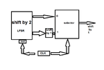
Well it might be possible to create an lfsr structure that produces two bits of the operation in one clock cycle. Then shift the lfsr by two bits instead of 1 to insert the two bits. A second parallel register just loads the 1 bit shifted data (or just the serial output bit). At this point you would used the clock as the select line to a mux to select the correct bit.

The problem with this type of design is you'll have glitches on the output at the clock transitions due to differences in delays. As mrfibble suggests just use a PLL/DCM to double the clock frequency and your problem becomes simple and you won't have to figure out how to avoid detecting glitches in downstream logic.
 
mrflibble :
The general idea is, did you actually read the thread? FvM's last post pretty much sums it up. So how are you planning to transpose that trick to the lfsr problem domain? What's that you say? eehhrrr, uhm, welllllll? exactly.

i am not a professional in vhdl and just a beginner so may be my idea is soo bad,but i think the implementation of dual LFSR will be like counter code

for FVM i really not understand what he mean.

- - - Updated - - -

Well it might be possible to create an lfsr structure that produces two bits of the operation in one clock cycle. Then shift the lfsr by two bits instead of 1 to insert the two bits. A second parallel register just loads the 1 bit shifted data (or just the serial output bit). At this point you would used the clock as the select line to a mux to select the correct bit.
.
i think this the idea like the counter i will try it now,
but what do you mean by glitches >???
regrads
 

the clock and the data (output of the lfsr and the 1 clock bit) will have skews associated with them. This skew will result in the arrival of the signals to the multiplexer being different, which could result in very narrow pulses (glitches) being produced during the switch between the two outputs.

e.g.

Suppose A switches from low to high at a clock edge and B is low both before and after the clock edge. If the mux select switches the output from A to B input then if the switch is early no glitch if it's late glitch.

if C == 0 selects A..

C A B O
0 0 0 0
1 0 0 0
1 1 0 0
we are good.

C A B O
0 0 0 0
0 1 0 1 <==== GLITCH!
1 1 0 0
we've got a potential problem
 
dear mrflibble
double.png
this is an idea to implement the LFSR
and this is a simple code i made it 4 bit LfSR like the counter code
this code is complete and this a simulink
lfsrworkwith rising and failling.png
library IEEE;
use IEEE.STD_LOGIC_1164.ALL;
use IEEE.STD_LOGIC_ARITH.ALL;
use IEEE.STD_LOGIC_UNSIGNED.ALL;

entity lfsr is
port ( rest,clk :in std_logic;
output :eek:ut std_logic_vector(3 downto 0) );

end lfsr;

architecture Structural of lfsr is
signal temp :std_logic_vector(3 downto 0):=(others=>'1');
signal temp2:std_logic_vector(3 downto 0):=(others=>'1');
begin
process (clk)
variable r:std_logic_vector(3 downto 0):=(others=>'1');
variable r2:std_logic_vector(3 downto 0):=(others=>'1');
variable t:std_logic:='0';
begin
if (clk'event and clk='1') then --- shift by 2
t:=r(0) xor r(1);
r(2 downto 0):=r(3 downto 1) ;
r(3):=t;
-------------------------------
t:=r(0) xor r(1);
r(2 downto 0):=r(3 downto 1) ;
r(3):=t;
--------------------------------
t:=r(0) xor r(1);
r2(2 downto 0):=r(3 downto 1) ;
r2(3):=t;

end if;
temp<=r;
temp2<=r2;
end process;

output <= temp when clk='1'
else temp2 ;

end Structural;

end Structural;

- - - Updated - - -

the clock and the data (output of the lfsr and the 1 clock bit) will have skews associated with them. This skew will result in the arrival of the signals to the multiplexer being different, which could result in very narrow pulses (glitches) being produced during the switch between the two outputs.

e.g.

Suppose A switches from low to high at a clock edge and B is low both before and after the clock edge. If the mux select switches the output from A to B input then if the switch is early no glitch if it's late glitch.

if C == 0 selects A..

C A B O
0 0 0 0
1 0 0 0
1 1 0 0
we are good.

C A B O
0 0 0 0
0 1 0 1 <==== GLITCH!
1 1 0 0
we've got a potential problem

dear ads_ee :
can we calculate optimum frequency to avoid this problem ??? or any suggestion
 
Last edited:

You can also differentially encode the data (output is the xor two registered outputs). In this case, you can use the LFSR property that (x[n] xor x[n+k]) will create the same lfsr sequence, but with a different offset.

Basically, you could just have two LFSRs and xor the output:
rising init 001. sequence = 0010111 (repeats)
falling init 111. sequence = 1110010 (repeats)
combined output, R/F/R/F/R/F/... = 01 01 11 00 10 11 10 = 0101110 (repeats)

It isn't too hard to get a specific alignment:
rising init 110. sequence - 1100101
falling init 111. sequence - 1110010
(111 xor 110 = 001) xor'd = 0010111

you can also create the "shift-by-two" version of the lfsr and do something similar.
 
I have no doubt it will look "okay" in simulation. This sort of thing always looks pretty in simulation. ;-)

The problems start when you implement it in real hardware. As ads_ee pointed out, you will have clock skew to deal with. Because some of your logic is fed with CLK, and some logic is fed with the inverted CLK. And since we are now talking about real hardware, where does this inverted clock come from? That will depend on the fpga you're working...

Say on for example you are using a spartan-3. That means you will have to do the clock inversion with a DCM, and you will have to use up an extra global clock net. Global clock nets are a relatively scarce resource, so you don't want to use them for every little thing. Apart from the use of a global clock net you now have quite a bit of skew to deal with. That inverted clock is a newly generated clock signal and will have associated jitter (clock uncertaintly). That jitter will have to be taken into account during timing constraints. Short version: this jitter will effectively lower the maximum frequency you can reliably run on.

For a spartan-6 things are a little better. You have local clock inversion, which means that you route only 1 clock signal (CLK). Then whenever you need the inverted version there's a tiny bit of dedicated hardware that inverts the clock signal on the spot. You can read the datasheet for more details... The good news is that you now only need 1 clock net instead of 2. The bad news is that you still get all sorts of challenges. Becaaaaaaaause your clock signal will not have a perfect 50% duty cycle. And because of that you get timing mismatches between CLK and NOT CLK. Essentially the same problem as with the jitter example earlier on. And as such in reality you will get a lower running frequency than you would have for a perfect 50% duty cycle.

So I am not saying it cannot be done. Because ... it can be done. But it does require more work to setup the constraints carefully to make sure that it will work reliably. And you may not be gaining any advantages over the regular boring 1 clock only case without inversions. So what is the design goal here? Just having fun and seeing if it can be done? In which case have at it! Try to get to run it near the rated max clock of your chosen fpga, and then double that by doing it the DDR way. That way you'll get to see all the fun stuff that can go wrong. :)

If you want something that "just works" then generating a X2 clock and using that is a lot safer. And not in the least because the synthesis and place & route tools have been optimized for the sort of circuit with a boring single clock. As soon as you stray from the synchronous logic path you will have to do more thinking yourself to make sure things don't go wrong.

You say you just started out with VHDL. If you currently have some spare time to look into how to properly constrain a design, I would say go for it. You'll learn lots of handy stuff.
 
You can also differentially encode the data (output is the xor two registered outputs). In this case, you can use the LFSR property that (x[n] xor x[n+k]) will create the same lfsr sequence, but with a different offset.

Basically, you could just have two LFSRs and xor the output:
rising init 001. sequence = 0010111 (repeats)
falling init 111. sequence = 1110010 (repeats)
combined output, R/F/R/F/R/F/... = 01 01 11 00 10 11 10 = 0101110 (repeats)

It isn't too hard to get a specific alignment:
rising init 110. sequence - 1100101
falling init 111. sequence - 1110010
(111 xor 110 = 001) xor'd = 0010111

you can also create the "shift-by-two" version of the lfsr and do something similar.

thank you allot

- - - Updated - - -

I have no doubt it will look "okay" in simulation. This sort of thing always looks pretty in simulation. ;-)

The problems start when you implement it in real hardware. As ads_ee pointed out, you will have clock skew to deal with. Because some of your logic is fed with CLK, and some logic is fed with the inverted CLK. And since we are now talking about real hardware, where does this inverted clock come from? That will depend on the fpga you're working...

Say on for example you are using a spartan-3. That means you will have to do the clock inversion with a DCM, and you will have to use up an extra global clock net. Global clock nets are a relatively scarce resource, so you don't want to use them for every little thing. Apart from the use of a global clock net you now have quite a bit of skew to deal with. That inverted clock is a newly generated clock signal and will have associated jitter (clock uncertaintly). That jitter will have to be taken into account during timing constraints. Short version: this jitter will effectively lower the maximum frequency you can reliably run on.

For a spartan-6 things are a little better. You have local clock inversion, which means that you route only 1 clock signal (CLK). Then whenever you need the inverted version there's a tiny bit of dedicated hardware that inverts the clock signal on the spot. You can read the datasheet for more details... The good news is that you now only need 1 clock net instead of 2. The bad news is that you still get all sorts of challenges. Becaaaaaaaause your clock signal will not have a perfect 50% duty cycle. And because of that you get timing mismatches between CLK and NOT CLK. Essentially the same problem as with the jitter example earlier on. And as such in reality you will get a lower running frequency than you would have for a perfect 50% duty cycle.

So I am not saying it cannot be done. Because ... it can be done. But it does require more work to setup the constraints carefully to make sure that it will work reliably. And you may not be gaining any advantages over the regular boring 1 clock only case without inversions. So what is the design goal here? Just having fun and seeing if it can be done? In which case have at it! Try to get to run it near the rated max clock of your chosen fpga, and then double that by doing it the DDR way. That way you'll get to see all the fun stuff that can go wrong. :)

If you want something that "just works" then generating a X2 clock and using that is a lot safer. And not in the least because the synthesis and place & route tools have been optimized for the sort of circuit with a boring single clock. As soon as you stray from the synchronous logic path you will have to do more thinking yourself to make sure things don't go wrong.

You say you just started out with VHDL. If you currently have some spare time to look into how to properly constrain a design, I would say go for it. You'll learn lots of handy stuff.
-------------------------
dear mrflibble:
i did not know what can i say to you,
but their is a simple word that describe you replay
======================
AMAZING
++++++++++++++++++++++

you open to my new doors and work so *** bless you
also i think i must Review myself and system
I have to study the terms jitte,skew8-O8-O in depth and see what they hidden And the problems that associated with them

so i think the best solution now is only to increase the frequency use dcm onl:|y.

also to answer your question which is what is the design goal here?

the goal is only to make this circuit execute for full period of 17 bit LFSR as fast as possible ,mean for (2^17)-1 clock with minimum time on fpga(spartan 3e exactly)

SYSTEM.png
 
Last edited:

Status
Not open for further replies.

Part and Inventory Search

Welcome to EDABoard.com

Sponsor

Back
Top