Continue to Site

Welcome to EDAboard.com

Welcome to our site! EDAboard.com is an international Electronics Discussion Forum focused on EDA software, circuits, schematics, books, theory, papers, asic, pld, 8051, DSP, Network, RF, Analog Design, PCB, Service Manuals... and a whole lot more! To participate you need to register. Registration is free. Click here to register now.

HV inverter switching noise affecting gate voltage

Electrowizard

Newbie level 5
Joined
Aug 3, 2023
Messages
8
Helped
0
Reputation
0
Reaction score
0
Trophy points
1
Activity points
54
Hello,

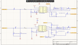
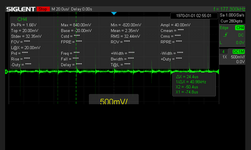
I am building a high voltage inverter operating at 200v. i am using isolated gate drivers and the supply for the gate drivers (15V) is also isolated. But the inverter switching causes a voltage spike in the gate driver power supply . the spike is happening at 40khz which is twice the switching frequency of the inverter. I have dc link capacitors and mlcc filtercaps attached to the dc line

Can someone help me figure out why the inverter switching noise is propagating to the low voltage side.

Thank you
 
Some images showing the "spikes" would be very helpful. And a simple schematic, showing how you are probing the circuit when you see the spikes.

First thing to rule out is the spikes being a result of bad probing.
 
The schematic is the gate drive . Im supplying the 15v through a pushpull configuration. when the inverter is not switching, there is no voltage spikes.when the inverter is switching , it induces a 40khz spike in the gate drive power supply which causes the gate voltage to the igbt to reach dangerous levels.

PS i have the power supplies for the gate driver in a different board ( LV board with the mcu ) and the gate drivers are present on the HV board mounted on top of the igbt . Power supply is given to the gate drivers through connectors
SDS00001 (1).png
 

Attachments

  • gd.png
    gd.png
    147.5 KB · Views: 59
So you're observing these spikes on the input side of the isolated drivers? Could be parasitic capacitance in the isolation transformers. Are they off-the-shelf power supplies, or custom?

The schematic you attached isn't legible...
 
also - most of those " spikes " are common mode " CM " pickup due to poor probing techniques

try shorting the probes on the pos rail and then the neg rail and see if the same " spikes " are there - if they are

think about your probing.
--- Updated ---

Is there a diode in your high side power feed ?

the complete and LEGIBLE schematic would be helpful
Attached the power supply and gate schematic.

Pos and neg rail meaning should i probe the power supply to the isolation transformer?

Thanks for the reply
 

Attachments

  • Gate drive circuit.rar
    67.7 KB · Views: 61
So you're observing these spikes on the input side of the isolated drivers? Could be parasitic capacitance in the isolation transformers. Are they off-the-shelf power supplies, or custom?

The schematic you attached isn't legible...
Its a custom power supply. Im not observing the spikes on the 5v input of the gate driver. Only the 15v side is affected

Thanks for the reply
 

Attachments

  • Gate drive circuit.rar
    67.7 KB · Views: 55
yes, yes, SHORT the scope probe on the +ve 15V rail, i.e. probe tip and gnd on this point

do the same on the 0v of the 15V supply

if you still see the spikes ( you should see zero - as the probe is shorted ) then the problem is in common mode noise - and the spikes are artifact only.
 
The dc/dc transformer (Pulse PH9400.111 ANLT) is specified with 45 pF winding capacitance. It's hard to avoid severe common mode noise with this large capacitance.
 
I would not take anything for granted, including the realism
of what's displayed. That kind of spiking / ringing can come
from instrumentation (like probe clip loop area). I'd spend
some effort at cleaner instrumentation. For example find
a probe tip with co-located ground prong to make loop
area infinitesmal. Maybe make a resistor divider that has
Zout=50 and run coax to the 'scope, for anything low-Z
(like a power rail). Cap-blocked divider for any flying high
side signals.

Your ground is going to get banged every main clock edge.
Got to deal.

Zoom way in on the action and see if the spiking comes
from the ground referred (via ground?) or the isolated
section, by the time-of-arrival (like, less than 1/4 the prop
delay total, probably is front end and half or more, likely
the back end polluting itself (weak fly cap?).
 
yes, yes, SHORT the scope probe on the +ve 15V rail, i.e. probe tip and gnd on this point

do the same on the 0v of the 15V supply

if you still see the spikes ( you should see zero - as the probe is shorted ) then the problem is in common mode noise - and the spikes are artifact only.
i shorted the probe at the 15v rail and im observing the 40khz spike
 

Attachments

  • cmnoise.png
    cmnoise.png
    77.6 KB · Views: 47
Attached the power supply and gate schematic.

Pos and neg rail meaning should i probe the power supply to the isolation transformer?

Thanks for the reply
Its a custom power supply. Im not observing the spikes on the 5v input of the gate driver. Only the 15v side is affected

Thanks for the reply
Ok now we get some more details.

Are you observing this on the supply for the high side driver, or the low side driver, or both?

What sort of probe(s) are you using to make these measurements?
 
OK - so the spikes are pure CM - due to setup and measurement " method "

just artifact, not real, a simple way to know this is to calculate the current required to lift a cap so many volts in so many nS

if the current is ridiculous then it is likely not real, for example, 10uF MLCC, 20V spike with a rise time ( or fall time ) of 20nS, I = C. dv /dt = 10uF. 20V / 20nS = 10,000 amps - is this likely ? answer = not.
 
Ok now we get some more details.

Are you observing this on the supply for the high side driver, or the low side driver, or both?

What sort of probe(s) are you using to make these measurements?
Observing this in both high and low side driver.
Im using normal oscilloscope probes (non isolated ) but im powering the oscilloscope from a battery powered UPS disconnected from the laboratory power liines
 
Do you know about CM ( common mode ) noise and how it increases as your voltage rail goes up ?
 
Do you know about CM ( common mode ) noise and how it increases as your voltage rail goes up ?
when i increase the dc voltage for the inverter , the amplitude of the spike goes up as well, is there a way i can eliminate common mode noise with any CM chokes or is board redesign required?
 
it is partly / mostly to do with probing technique, heat-sinking of semi's (capacitance to an aerial ), and speed of turn on - hard to explain without seeing everything 1st hand
 

LaTeX Commands Quick-Menu:

Similar threads

Part and Inventory Search

Welcome to EDABoard.com

Sponsor

Back
Top