Continue to Site

Welcome to EDAboard.com

Welcome to our site! EDAboard.com is an international Electronics Discussion Forum focused on EDA software, circuits, schematics, books, theory, papers, asic, pld, 8051, DSP, Network, RF, Analog Design, PCB, Service Manuals... and a whole lot more! To participate you need to register. Registration is free. Click here to register now.

DC-DC output voltage dropping due to RF noise

biswaIITH

Full Member level 4
Joined
Aug 23, 2014
Messages
204
Helped
27
Reputation
54
Reaction score
28
Trophy points
1,308
Location
Hyderabad
Activity points
2,907
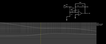
We are facing an issue where the output of the DC-DC(12V) drops to 1-2 V for few milliseconds when an SOM module tries connecting with the cloud. The DC-DC is designed using LM5146 IC from texas instruments

This is mostly due to RF noise we suspect.
Can anyone suggest any shielding technique to prevent the above?
 
Solution
What is the power source for the DC/DC converter ? - if this cannot supply the power needed by the system ( 140 W by your estimate at full power ) the you will have the issues you are seeing.
Hi,

voltage of a power supply usually drops because of current.
But you don´t give any information about available and drawn current.

.. and you say "just for a few ms" ... this makes no sense if the cause is "RF noise".

--> measure the current.

****
But fur sure RF noise my have some influence on the regulation loop.

Also you say it is made with a LM5146 ... But no information if this is a proper design following the ruels of the datasheet, or is it some tinkerer design.

--> provide all necessary informations.

Klaus
Yes the design is done as per the datasheet even reviewed by the TI design experts.

The dc dc is designed for 13.8V,10A . The voltage drops even when the load is less than 3-4 A when the SOM module trying to connect with clound under low coverage area such as a basement.
Even we have checked the stability of the control loop which has a PM roughly around 45 degrees

Initially we thought it to be a over current issue & We have done the transient load analysis giving ( 0-10)A under which the voltage drops by hardly 1.5V.
 
Pleas do following load transient step analysis...
1....Put SMPS on no load.
2...Then very suddenly, using a fast switching mosfet, switch on a 10A load to the output.
3...Then report back what is the voltage undershoot at the output.

Only do the one load step, do not have the load steps continuously going on/off at high frequency.

Be sure to take the scope after any output filter inductors, not before.
_____________________________ ___
Are you sure the pulse of current drawn by the radiO module is mess than 10A?
____________________________ ____))--((____ ____________________________________
Also, i will send you PCB layout doc for SMPS.
 
Can you duplicate the dip with a step load pulse such as an NPN sink and measure the load regulation error (dynamic and static).

Then report values for these components.
1706982937463.png
 
I have glanced at a bit its datasheet. It's pretty critical to design a well working regulator.
Especially components' specifications and design tricks are sensitive. For instance low ESR, high quality Elco Capacitors are needed to prevent transient load currents. Even the layout should be carefully designed.
 
What is the power source for the DC/DC converter ? - if this cannot supply the power needed by the system ( 140 W by your estimate at full power ) the you will have the issues you are seeing.
 
Solution
What is the power source for the DC/DC converter ? - if this cannot supply the power needed by the system ( 140 W by your estimate at full power ) the you will have the issues you are seeing.

SOM needs hardly 10-12 W of power . As I had mentioned earlier , DC-DC is working properly under all operating conditions. Except for when SOM is trying establish communication under low network area.

Should I add some extra Phase margin to the DC-DC converter control loop,???
 
Should I add some extra Phase margin to the DC-DC converter control loop,???
I don´t think extra phase margin improves the situation, if external HF is the problem.


so I guess you designed it on yor own.

Show us your schematic and PCB layout.

Klaus
 
1707049128806.png

I don´t think extra phase margin improves the situation, if external HF is the problem.


so I guess you designed it on yor own.

Show us your schematic and PCB layout.

Klaus
Which component is getting impacted ??? Is it the main IC or the COMP pin?

A bit of modification... Switching frequency is 100Khz in the actual design.

EN pin of the IC is pulled up to Vin_FLT with a pull up resistor.
 
Does anyone see any problems with this Feedback gain and slope?
I would significantly reduce the 24k to boost error-correction gain in the <1ms pulse range.

1707062050519.png
 

Attachments

  • 1707062033634.png
    1707062033634.png
    335.3 KB · Views: 51
Last edited:
Hi,

there are 0603 capacitors 100nF/100V. What ceramics type are they?

A clear mistake: see Fig 11-1 of the datasheet. The capacitor for VCC needs to refer to PGND (not AGND). Thus in your case all the gate drive current needs to use a high impedance detour via AGND, the tiny connection between AGND and PGND, then to the MOSFET.

Show us your schematic and PCB layout.


Klaus
 
Some op amps make a feature of RF rejection (like ones too slow to
respond to it?).

But I see nothing besides the original assertion that RFI is the cause.
Crossing up analog and power grounds seems like a thing to fix
before concerning yourself with subtleties.
 
Hi,

there are 0603 capacitors 100nF/100V. What ceramics type are they?

A clear mistake: see Fig 11-1 of the datasheet. The capacitor for VCC needs to refer to PGND (not AGND). Thus in your case all the gate drive current needs to use a high impedance detour via AGND, the tiny connection between AGND and PGND, then to the MOSFET.


Klaus
1707142258357.png


It is a bit confusing. Coz in another page it is mentioned to connect to AGND.
 
Because it does not appear to be set up as proper current mode - more RC damping on the output caps - and extra damping in the control loop would be highly beneficial - also having a crossover freq ( gain = 0 dB ) for the control loop at 10x less than the Fo of the output filter would help greatly with stability !
 

LaTeX Commands Quick-Menu:

Similar threads

Part and Inventory Search

Welcome to EDABoard.com

Sponsor

Back
Top