Welcome to our site! EDAboard.com is an international Electronics Discussion Forum focused on EDA software, circuits, schematics, books, theory, papers, asic, pld, 8051, DSP, Network, RF, Analog Design, PCB, Service Manuals... and a whole lot more! To participate you need to register. Registration is free. Click here to register now.
Hi! I want to simulate AND operation using MOSFET's in Proteus. I have attached a screenshot of the design. But I'm not getting the necessary output. (when A and B is logic 1 Z should be logic 1) What is the mistake?
The circuit seems to be correct. I just tried interchanging the components bt still the result is same. I'm not sure whether I choose the correct MOSFET.
- copy a CMOS AND gate from literature
- derive the circuit respectively correct a wrong approach based on known behaviour of MOS transistors
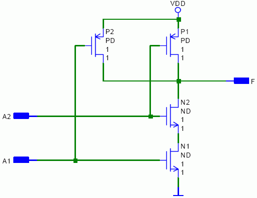
Presently I'm under the impression that you have difficulties with either method. Please compare your circuit (without the inverter) little-by-little with the below shown copy from an ASIC library. Pay attention to the letters "N" and "P" and the position of source terminals.
To be honest, the position of source terminals doesn't actually matter because source and drain are interchangeable. But the MOS transistors used in your simulation have source and substrat terminal shorted against each other, and the substrate connection definitely matters. In a standard CMOS process, all N substrates are connected to GND and all P substrates to VDD. To model it exactly, you would use transistor symbols with separate substrate connection.
Thanks for the reply FVM. I do not want to use the MOSFET with substrat terminal. Since I couldn't find a typical MOSFET I used this. It would be better if I could find it in Proteus.
This site uses cookies to help personalise content, tailor your experience and to keep you logged in if you register.
By continuing to use this site, you are consenting to our use of cookies.