Continue to Site

Welcome to EDAboard.com

Welcome to our site! EDAboard.com is an international Electronics Discussion Forum focused on EDA software, circuits, schematics, books, theory, papers, asic, pld, 8051, DSP, Network, RF, Analog Design, PCB, Service Manuals... and a whole lot more! To participate you need to register. Registration is free. Click here to register now.

How to obtain the I-V curve to check the size effect of PMOS pass transistor in LDO?

Status
Not open for further replies.

roki

Member level 1
Joined
Mar 29, 2009
Messages
33
Helped
0
Reputation
0
Reaction score
0
Trophy points
1,286
Activity points
1,545
Hi,

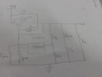
I want to simulate an I-V curve wrt to different sizes of my PMOS pass transistor to see its functionality. But i am not sure whether i am even doing the correct way.
2012-09-15 00.38.59.jpg

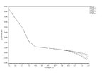
So from the figure, in order to get Id vs Vds curve, I gave two DC source,VGS of 0.5V and VDS of 0.3V (located near the PMOS pass transistor). Then i sweep VDS with the intention to get the Id vs VDS curve. I run this for 4 different pass transistor sizing. But i graph i got is so weird that i believe what i did maybe completely crap.
ESR pass transistor i vds.jpg

Please guide me in obtaining the correct ans.

Thanks

Regards
 

Looks like it's just upside down.

There are two things you need to look at and they don't even
need a curve.

One, your on-resistance times max rated current has to be
below dropout voltage spec at the minimum working voltage's
applied Vgs to the pass FET. This includes error amp headroom
and to remain stable and in regulation, you need some linear-
range margin in that budget as well.

Two, your minimum-rated-load current at maximum input
voltage, minimum output voltage has to be supported. There
are similar headroom constraints, you can't have a linear
error amp and zero Vgs on the pass FET without some
higher supply potential, which cannot always be assumed -
asserted, if you're in control of the datsheet, but it won't
be real broad-application-friendly.

Last, the shutdown leakage current with a true (near-)
zero Vgs has to be met.

So you really just need three DC OP results (and a model
that represents the FET's behavior and variations well).

If you're doing a ~1A LDO, you should target half of the
advertised dropout (on-resistance*Iload) for the FET and
allocate the remainder to interconnect, bond wires and
package.
 

Hi dick_freebird,

Just for clarification, so did the method i used to get Id vs Vds curve acceptable?
While it appears to be upside down,hmm.... i still think it is wrong.
Because the Id axis value doesnt come close to the value i've checked through DCOP of pass FET.
Well since it is a PMOS, the Id and vds value is expected to be a negative value.
Is there a better way to generate a more proper curve?

Pardon me, based on your explanation, i still dont catch the concept or the relation with regard to the effects of using different sizing of pass FET.
May i know whether the explanation stated is some sort like a requirement to ensure the pass FET is working?
Sorry, my foundation in analog isnt strong.
 

I want to simulate an I-V curve wrt to different sizes of my PMOS pass transistor to see its functionality.

... in order to get Id vs Vds curve, I gave two DC source,VGS of 0.5V and VDS of 0.3V (located near the PMOS pass transistor).
Then i sweep VDS with the intention to get the Id vs VDS curve. I run this for 4 different pass transistor sizing.

Hi roki,

I think it's better to give a fixed Vin (e.g. 0.3V more than required Vout), leave the necessary VGS to the error amplifier, then sweep the load current up to your requirement, and do a 2nd sweep over W of the pass transistor, run a DC analysis with these 2 sweeps and plot Vout vs. i_load, s. this PDF:
 

Attachments

  • LDO_2.pdf
    32.2 KB · Views: 106

Hi erikl,

Thank you for showing me an alternative way. I've tried to running it. I did manage to sweep the load current.However, i am facing a problem where i cant sweep the W of the pass transistor. It keeps having this error where it doesn't recognise my pass transistor.=( I'm not sure why. I have tripple check my sweep setting, but does not justice at all.
Please help.
Thanks.
 

Hi roki,

would you mind revealing which simulator environment you're using? Not all simulators are able to run multiple sweeps.
 

I am using mentor graphics eldo 0.13micron, SPICE model
 
Last edited:

I am using ... SPICE model

I'm not sure if SPICE can master 2-dimensional sweeps. Show your control file! Perhaps somebody can help you.
 

Status
Not open for further replies.

Part and Inventory Search

Welcome to EDABoard.com

Sponsor

Back
Top