Continue to Site

Welcome to EDAboard.com

Welcome to our site! EDAboard.com is an international Electronics Discussion Forum focused on EDA software, circuits, schematics, books, theory, papers, asic, pld, 8051, DSP, Network, RF, Analog Design, PCB, Service Manuals... and a whole lot more! To participate you need to register. Registration is free. Click here to register now.

how to match impedance for DP ? how to choose the trace width for DP matching ?

Status
Not open for further replies.

kabaleevisu

Advanced Member level 2
Joined
Apr 14, 2010
Messages
616
Helped
85
Reputation
170
Reaction score
81
Trophy points
1,308
Location
Chennai,India
Activity points
4,512
hi all ,

i have the board file which containt impedace 50E ,90E ,100E , for differential pair trace width is kept as 4.5 mil i have some clarification about impedance matching

1.how to choose the trace width for impedance 50E ,90E ,100E ??
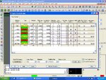
2. setup --- > cross section impedance is change when i changing trace for example i choose 100E trace width is (for differential pair )0.502mil only but in constraint manager kept as (for differential pair ) 4.5mil ,how it is come ?? i could not understand
3.what is reason to choosing negative artwork only in plane layer

please give me the suggestion to me


Attachments

  • cmgr.JPG
    cmgr.JPG
    169.6 KB · Views: 77
Last edited:

1. There are many tools(ex: polar) available for impedance calculation. Please get the trace width for your 50E,90E and 100E diff signals and add use this for the respective signals
2. Choosing negative artwork for planes is bad . use the positive planes so that we can see the area of planes. But if you select the negative planes you will not see anything . (Ex. Mask is a negative artwork layer. So in PCB if you have the pad on mask layer you will not get mask in that area on the PCB after fabrication


Thanks
Rajan
 

thanks for your reply ,

what is the reason to choosing negative in plane layer ??
please the image
 

the advantage of reducing negative plane layer is by doing so the size of files reduces. It also helps in large boards, as positive planes takes time to refresh every time some modifications are done.
 

Most people lay out the board with planes set to negative, then turn the planes to positive when the signal routing is done. This gives optimum speed when routing and positive planes for final DRC's etc.
 

hi all,

how i will do the placement of this board here i attached the placement is it ok

i have certain doubt in placement please clarify any one

how can i place 512K-Bit SPI EEPROM, Flash memory in this board how many distance from processor?which one come first after the processor? (because length matching is considered ) this placement ok


Placement seems to be OK. but the it depends of your requirement. place the memory and usb near to the processor . because it is high speed..

Regards
praveen Bhat
 

thanks praveen
which one come first 512K-Bit SPI EEPROM or flash memory because address and data present in flash memory so need to length match right and another one doubt is BGA is 0.65mm pitch how to select via for fan out (dog bone) please reply
 

Thanks praveen ,
what is Xnet ?
GPIO signal is going from processor to connector , switch and another connector , it is need to length match so need T Point how to create T point ?
what is the use of Net class compare to bus ??
 

xnet is used creating model for topology routing for DDR2..An XNet is an extended net, typically a net, a series resistor and another net would combine as an XNet between two pins. A differential pair would be two independent nets carrying a complementary signal to improve signal quality, typically matched in length and routing topology, these differential pair nets might be XNets. See the discussion on Extended Net in the Allegro PCB SI User Guide.

**broken link removed**
 

Status
Not open for further replies.

Part and Inventory Search

Welcome to EDABoard.com

Sponsor

Back
Top