Continue to Site

Welcome to EDAboard.com

Welcome to our site! EDAboard.com is an international Electronics Discussion Forum focused on EDA software, circuits, schematics, books, theory, papers, asic, pld, 8051, DSP, Network, RF, Analog Design, PCB, Service Manuals... and a whole lot more! To participate you need to register. Registration is free. Click here to register now.

50ohm Impedance for Coplanar Strips

m.charge

Newbie level 5
Joined
Nov 10, 2013
Messages
8
Helped
0
Reputation
0
Reaction score
0
Trophy points
1,281
Activity points
1,341
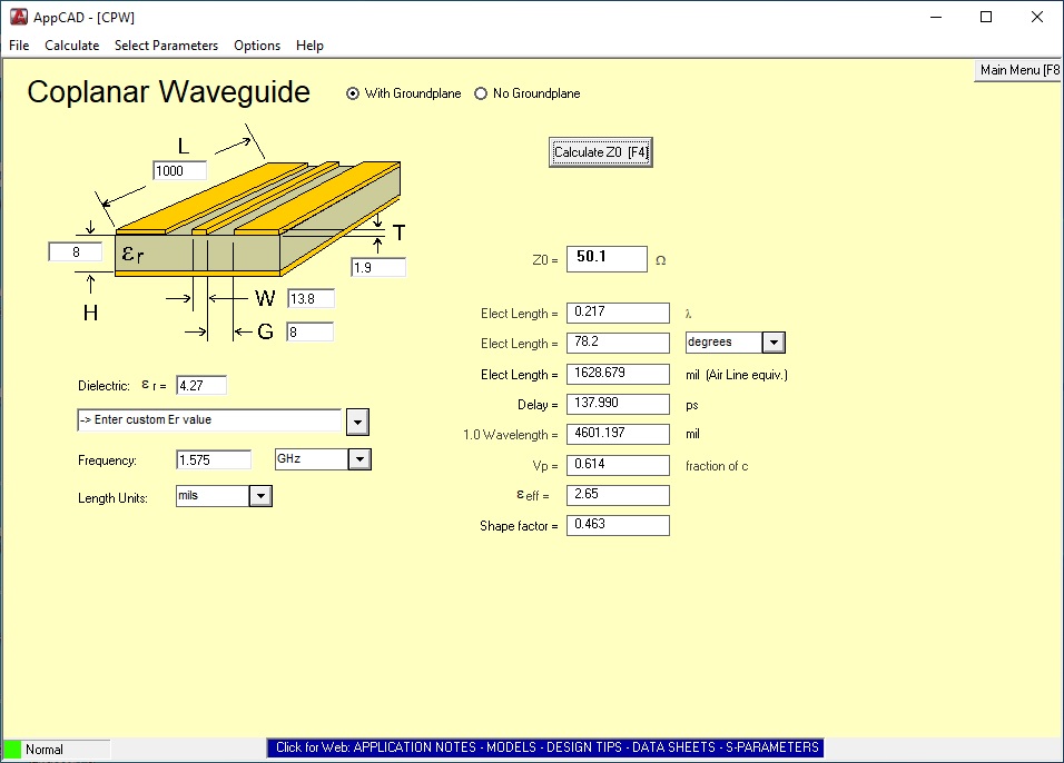
I need some help to decide about the way I'm designing the circuit to achieve the best antenna performance while meeting the 50ohms impedance for the transmission line, in the first example below, I made the line width 10.7 mil and the gap equal to 5 mil, on the second example, the line width changed to 13.8 when the gap increased to 8 mil, I can achieve the 50 ohms on both examples, knowing that I got the H, T and the ER values from the board house so I'm only focusing on the W and G widths, I'm designing for the frequency range of 700 MHz to 2.5 GHz, my questions:

1. Which way is preferred? increasing the line width or increasing the gap width?

2. I've been told that G value must be equal to H value, but I am not sure how true that is!

3. Does dielectric thickness H is important for the RF performance? is 4.3 mil acceptable? or should it be okay as long as I can design the circuit for the 50 ohms impedance?

Your help is highly appreciated.

TL 1.jpg


TL 2.jpg
 
1. Real PCB have trapezoidal rather than rectangular trace shape due to etch process. Simulation tools should be aware of and provide an etch factor or separate width parameters. AppCad apparently doesn't, the results for 5 mils gap can't be expected to match final PCB impedance well.

Even if trace shape is modelled correctly, gap width near technology minimum for 1 oz copper will vary considerably in production. Therefore wider trace + gap can be expected to give better matching in production.

Generally, it's important to realize the limititations of designed impedance compared to impedance controlled PCB production. The latter involves test structures in PCB, sample impedance measurement and parameter tuning during production. Expect at least +/- 10 % variation of designed impedance.

2. Extreme W/H ratios will reduce the accuracy of simplified impedance calculation methods used by most tools, surely it must not be 1.0 specifically

3. Not particularly. If you want RF performance, you'll chose RF PCB substrate rather than FR-4.

1699947046371.png
 
Last edited:
Very thin substrates give extreme W and G values. You should use a thicker substrate because manufacturing tolerances can be very troublesome.
1.57mm substrate thickness is fine for 0.7-2.5GHz band unless there is a particular reason.
 
1. Real PCB have trapezoidal rather than rectangular trace shape due to etch process. Simulation tools should be aware of and provide an etch factor or separate width parameters. AppCad apparently doesn't, the results for 5 mils gap can't be expected to match final PCB impedance well.

Even if trace shape is modelled correctly, gap width near technology minimum for 1 oz copper will vary considerably in production. Therefore wider trace + gap can be expected to give better matching in production.

Generally, it's important to realize the limititations of designed impedance compared to impedance controlled PCB production. The latter involves test structures in PCB, sample impedance measurement and parameter tuning during production. Expect at least +/- 10 % variation of designed impedance.

2. Extreme W/H ratios will reduce the accuracy of simplified impedance calculation methods used by most tools, surely it must not be 1.0 specifically

3. Not particularly. If you want RF performance, you'll chose RF PCB substrate rather than FR-4.

View attachment 186218
- Do you recommend any App/ tool for impedance calculation that has accurate results? I used the Polar Si8000 before but I didn't have a budget to purchase the license

- What kind of substrate do you recommend?

Thanks
--- Updated ---

Very thin substrates give extreme W and G values. You should use a thicker substrate because manufacturing tolerances can be very troublesome.
1.57mm substrate thickness is fine for 0.7-2.5GHz band unless there is a particular reason.
Due to the via in-pad process, the board house suggests using the 4.3 mil substrate, I am not sure if this is something I need to worry about.
 
Last edited:
Due to the via in-pad process, the board house suggests using the 4.3 mil substrate, I am not sure if this is something I need to worry about.

Approx. 0.1mm thickness is a real trouble for RF circuits.
What is " Via in Pad" process ?? Why this brings a particular constraint ??
 
Due to the via in-pad process, the board house suggests using the 4.3 mil substrate

Sounds like laser-drilled micro via. 50 ohm designed impedance with 4.3 mil substrate is o.k. for digital and mixed signal multi layer accepting respective impedance tolerances, but not for dedicated RF PCB with tightly tolerated impedance.

The PCB requirements aren't completely clear, I'm under the impression that you are trying to combine incompatible technlogies.
 

LaTeX Commands Quick-Menu:

Part and Inventory Search

Welcome to EDABoard.com

Sponsor

Back
Top