Continue to Site

Welcome to EDAboard.com

Welcome to our site! EDAboard.com is an international Electronics Discussion Forum focused on EDA software, circuits, schematics, books, theory, papers, asic, pld, 8051, DSP, Network, RF, Analog Design, PCB, Service Manuals... and a whole lot more! To participate you need to register. Registration is free. Click here to register now.

How to isolate Vcc of a noisy chip?

Status
Not open for further replies.

blapcb

Full Member level 3
Joined
Jan 7, 2007
Messages
188
Helped
2
Reputation
4
Reaction score
0
Trophy points
1,296
Location
Planet earth (most of the time)
Activity points
2,766
The line drivers I am using (MAX3232) are injecting a lot of A/C ripple in to the 3.3v Vcc (about 80-100mV) because of their charge pumps. My LDO is MIC5209 and without the line drivers I get only 5-10mV ripple. How can I isolate the Vcc going to the line drivers from the rest of the rail? Some type of inline filter?

Thanks
 

you can use ferrite beads.
 

you can use ferrite beads.

How do I rate/specify the beads? And should I also use two capacitors before/after in order to form a pi filter? (and if so, how to rate them?).

Lastly, I have two such line drivers. Should I do this on each Vcc separately or one for a Vcc common to both?

Thanks!
 

No,
The capacitors aren't necessary. The bead acts more like a resistor for the high frequency spectrum of the signal.
You should choose one according to the current that you intend to pass through it and the frequency suppresion range.
 

No,
The capacitors aren't necessary. The bead acts more like a resistor for the high frequency spectrum of the signal.
You should choose one according to the current that you intend to pass through it and the frequency suppresion range.

Actually as I read about this, it seems that beads are only good for MHz range isolation. My noise is in the XXKhz range, so how can this work? Or am I not understanding something?
 

This is true.
FB are usually designed for high frequencies.
BUT, there's a reason to suppress noise at the MHz range - most of the electronic equipment works at high speed / low voltages where noise can have disruptive effects.
If your DC/DC generates noise in the KHz range, it has little effect on the signal integrity of your electronics - and doesn't radiate outwards very well.
I wouldn't bother suppressing it.

A tree that falls in the forest makes a lot of noise - but only if someone is there to hear it...
 

If your DC/DC generates noise in the KHz range, it has little effect on the signal integrity of your electronics - and doesn't radiate outwards very well.
I wouldn't bother suppressing it.

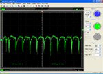
Well that is the issue. It does not affect the digital components, but it messes up a RF module which is fed from the same Vcc. That is the reason why I want to suppress it. Here is an image of Vcc at present:

MAX3232 Vcc.JPG
 

What is the frequency of the RF module?
 

What is the frequency of the RF module?

It is a 2.4GHz module, based on Nordic nRF24L01+

Quoting from one of their documents: "If these spikes reach the power pins of the RF part of the circuitry, serious malfunction might result. It is therefore mandatory to keep separate power lines to the analog and the digital domains of the circuit (star routing of VDD)."

Now, my board is a two layer board and I only have one Vcc (3.3v) from which this module is fed. Basically what happens is that some times when/if the noise is too much, the receiver on the module is messed up and does not work (we know this because while we still can communicate with the module over SPI and send data, nothing is received).
 

If the frequency is too low for a ferrite bead to be effective, then you will probably need an actual choke inductor on the supply rail, isolating the 3.3V supplying the MAX3232 from the RF supply. You want the cutoff of the LC formed by the MAX3232 bypass caps and the choke to be well below the the switching frequency (so maybe 100uF and a few uH of inductance). If this causes ringing, at its resonant frequency, then you can damp it by putting a resistor in parallel with the choke.
 

I advice to do the following:
Disconnect the DC/DC and power the circuit with an LDO for testing (just to make sure that the noise is the cause of the problem).
If the problem stops, and you can't live with a permament LDO - I would try adding a ferrite bead to see what happens.
Even if your DC/DC generates noise in the KHz range - some higher frequency harmonics might exist.
 

One thing to look at is the current loops of the charge pump
and output drivers, and whether your close-in decoupling is
shorting them effectively or shunting noise to where it has
no direct current return, and just contaminates something
else.

Look at the difference with the transmission line attached /
detached to get an idea of whether this is driver transition
related. Look at frequency to see if it's pump or driver or
both (likely, a HF from the pump which is modulated by
driver activity / makeup current demand).

See if you can determine whether noise is pushed into
ground and passed to Vdd by the decoupling. Look at
the power & ground, referred to the RF section ground,
and see which one is really the interferer (or both).
This might tell you where the ferrite ought to go.
 

I replaced the 0.1uF bypass cap with a 10uF one and it did help bring the noise down to a 10-15mV level. But, when the line is driving, this increases again by X2 or X3.

I was wondering, how about if I use a separate LDO only for the rail that goes to the RF module? Would that solve/help the problem?

I would add that I am presently looking for a fix that I can accommodate on my 2 layer board. While I would like to get this done in a 4 layer ("professionally") and also use components smaller than 1206 (to allow for closer coupling etc), this is not possible for the project at the moment. I know it is the better/proper approach, but can't be done just right now.

This is why I am shopping for a solution that will fix things well enough till the design/product is validated and just can justify the additional expense (and time).
 

Yes, I also increased the bypass cap on the MAX3232 to 10uF and that helped, but when you connect a RS232 device the problem increases. I want to try the series resistor thing but have to make a new PCB for that... but few people have suggested that also (10ohm with 10uF on either side).
 

I want to try the series resistor thing but have to make a new PCB for that... but few people have suggested that also (10ohm with 10uF on either side).

Please read it again carefully, because my main advice was to add a resistor to C1 and not (only) in the supply line. C1 is the flying cap of the first charge pump stage, that you connect between C1+ and C1- pins. Add a resistor of 47 ohms in series with that. You can try it without PCB modification, too (I made such an arrangement on the pads for C1: Λ)

For the second step, to add an C-R-C filter in the supply line you'll need to scratch off some track to accomodate the R, indeed.
 

You may consider a complete split of the analog and digital power supply and make sure that the digital switching current via ground is not flowing frought the analog ground. Here is an example of the separete supply for digital and analog: **broken link removed**

Enjoy your design work!
 

Status
Not open for further replies.

Similar threads

Part and Inventory Search

Welcome to EDABoard.com

Sponsor

Back
Top