Continue to Site

Welcome to EDAboard.com

Welcome to our site! EDAboard.com is an international Electronics Discussion Forum focused on EDA software, circuits, schematics, books, theory, papers, asic, pld, 8051, DSP, Network, RF, Analog Design, PCB, Service Manuals... and a whole lot more! To participate you need to register. Registration is free. Click here to register now.

how to determine noise figure and power consumption??urgent

Status
Not open for further replies.

jlim

Member level 1
Joined
Feb 19, 2013
Messages
40
Helped
0
Reputation
0
Reaction score
0
Trophy points
1,286
Activity points
1,549
Hello,

1. Could anyone help that how to determine noise figure and power consumption using cadence software for 013 technology??
2. How to draw the layout of capacitor in cadence??what is the name of instance of capacitor??

Thanks~~~
 

Hi everyone,

Could anybody teach me how to get the noise figure and power consumption of OTA-C filter for cadence 0.13um technology?? what analysis in cadence i can use and how to use the analysis??

Thanks~~~
 

You can find your current consumption by running a DC analysis. If you annotate the DC operating points the current will be displayed. Either use the current stated on the supply voltage source, or sum the currents of your current sources. Then your power consumption is simply P=Vsupply*I.

If a simple noise simulation will do, then follow this guide. https://eda.engineering.wustl.edu/wiki/index.php/How_to_Perform_a_Noise_Simulation_in_Cadence

If you really need to find the Noise figure then take a look here. https://www.edaboard.com/threads/16607/.

And search the forum. That way you could have easily found what you needed.
 
Last edited:

Using the method of the first link, if you replace V1 with a port (analogLib -> port) and set it as the input port for input noise simulation (at the noise analysis options) then it will also calculate the noise figure.
 

Thanks a lot for your reply and giving me the information...

1. But i don't understand abt the value in noise summary, what is the unit for the noise contribution?
2. If i want to get the waveform by having noise figure in dB, how can i do? is it possible i change the input voltage source to port from analogLib, but it does not have layout for the port source??
 

1. You can choose the unit in the main form panel. If you don't know what it means, check any analog design book and read about noise.
2. Noise figure is already given in dB when you plot it. No analogLib component has a layout view. You don't need it.
 

hmm~~~
What is your mean main form panel to choose the unit..?? Now i have do the noise analysis based on the link u given: https://eda.engineering.wustl.edu/wiki/index.php/How_to_Perform_a_Noise_Simulation_in_Cadence...
i get the result is like the attachment below..how i can know how much the noise figure (dB) in the circuit?

1.PNG


Thanks~~~ ;-)
 

You have to do: Results -> Direct Plot -> Main form -> noise analysis. Then choose noise figure and press plot. It will plot the NF in dB.
For the Output/Input noise you can choose the units you prefer.
 
  • Like
Reactions: jlim

    jlim

    Points: 2
    Helpful Answer Positive Rating
thanks for teaching me~~
But my target is about 40 dB for noise figure...it is a large different with the measured value about 144.42 dB (shown in attachment). How can i fix it and get my target value??
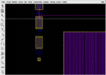
Besides that, i also have another question is about layout. If i want to connect capacitor layout fm3m1 (purple) with poly (gate of transistor), which metal i should use or how i can connect it??The attachement is shown below..

Thanks~~

n.PNG

https://mail-attachment.googleuserc...365740257618&sads=pJuH2Qoy6LAmxfKiK9VkRW6o28Q

- - - Updated - - -

thanks for teaching me~~
But my target is about 40 dB for noise figure...it is a large different with the measured value about 144.42 dB (shown in attachment). How can i fix it and get my target value??
Besides that, i also have another question is about layout. If i want to connect capacitor layout fm3m1 (purple) with poly (gate of transistor), which metal i should use or how i can connect it??The attachement is shown below..

Thanks~~

n.PNG

https://mail-attachment.googleusercontent.com/attachment/u/0/?ui=2&ik=44bee41193&view=att&th=13dee1892a44f457&attid=0.1&disp=inline&realattid=f_hfauyyi40&safe=1&zw&saduie=AG9B_P-QQZabC2sTCNRDZmLbsIYa&sadet=1365740257618&sads=pJuH2Qoy6LAmxfKiK9VkRW6o28Q
 

I cannot help you with the design issues. You should consult your text books.

I cannot see the layout picture, it doesn't matter thought. You should check the documentation of your technology for any special rules.
 

l.PNG

The attachment shows the layout of a part of my designed circuit..the purple is the layout of capacitor (fm3m1) and left one is NMOS transistor...How i can connect the capacitor with the poly (gate of NMOS)?? because i don't know what is metal inside the capacitor fm3m1 (purple)..
 

There is no way for me to know what metal layer is the purple one, I don't have this technology.
You should check you tech documentation.

Maybe "Design -> tap" can help you. Use Tap and select the capacitor metal. The appropriate metal should be chosen automatically at the LSW window.
 

Status
Not open for further replies.

Part and Inventory Search

Welcome to EDABoard.com

Sponsor

Back
Top