engrvip
Full Member level 2

- Joined
- May 3, 2006
- Messages
- 142
- Helped
- 3
- Reputation
- 6
- Reaction score
- 0
- Trophy points
- 1,296
- Activity points
- 2,377
How to source foll. BUFFER ckt. for CMOS CFA
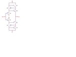
I am in process of designing a CMOS CFA ( current feedback amplifier ). And this is one of the buffer ckt architectures I have found from technical papers by C. Toumazou.
But I am not able to DC bias this ckt to provide sufficient operating current. Can somebody explain its functioning and sizing (W/L) procedure ?
Thanks
Vipul