Continue to Site

Welcome to EDAboard.com

Welcome to our site! EDAboard.com is an international Electronics Discussion Forum focused on EDA software, circuits, schematics, books, theory, papers, asic, pld, 8051, DSP, Network, RF, Analog Design, PCB, Service Manuals... and a whole lot more! To participate you need to register. Registration is free. Click here to register now.

Design 220VAC to 3.3VDC, how to prevent component shock

avner_g

Junior Member level 2
Joined
Nov 25, 2023
Messages
22
Helped
0
Reputation
0
Reaction score
0
Trophy points
1
Activity points
227
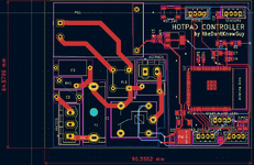
I am building an SMD soldering hot plate station. I got good results when prototyping this, using this guy, which is a 100x200 500W.
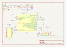
Since I am a novice, definitely in 220V, I wanted a hint on how to protect the components against bursts when the relay disconnects the hot pad.
I see some disturbances on the LCD on disconnections.
I thought of putting a veristor on the hot pad clamps, not sure what spec it should be (and if it is helpful).
Also, any other advice would be welcomed.
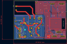
(Grounding of the hot pad is not illustrated here but is planned.)
1707840191316.png
 
Hi,

some recommendations:
* solid - I mean really "solid" - GND plane.
* a 100nF ceramics at every power supply pin of every IC
* no left floating inputs / IOs
* an RF filter between mains input and power supply
* an Y rated capacitor from mains_earth to your GND
* keep on safety regulations according creepage distance..
* keep all the mains circuits in a small area
* use proper pull up resistors at the I2C signals.

****

The heater will be resistive. I don´t expect high burst energy.
A snubber could be useful. I like varistors to keep peak voltage low.
And to keep your circuit stable when switching the heater ... mainly is a PCB layout problem.

Klaus
 
Thank you @KlausST for your quick replay.

I have implemented your feedback 1:1 to the best of my understanding, which means I might misunderstood something.
Not sure if the components I chose, mainly for both the verisitors, are the correct parameters, so I noted them on the plan
hoping to get your blessing.

Thanks!

1707916330089.png


1707935385637.png


1707935344612.png
 

Attachments

  • 1707935094010.png
    1707935094010.png
    382.6 KB · Views: 33
Last edited:
Here is an updated version of the board, with a greater clearance between the power lines.
main questions:
1. Are the components I chose for the power sections (RV1, C2, C3, FL1 and RV3) are going to do the job?
2. Are there any major errors in the PCB design?

thanks!!!
1708007567060.png

1708007480036.png
 

Attachments

  • 1708007532097.png
    1708007532097.png
    724.7 KB · Views: 33
* keep on safety regulations according creepage distance..
How much creepage distance do you need? I don´´t know your country and what standards do apply. But I guess its about 5mm.

How much do you have? maybe 0.5mm!!!!!

Don´t work with dangerous high voltage when you don´t know the regulations. You are likely to harm or kill yourself or others and you are fully resonsible for this.

Klaus
 
Hi,

do you know the difference between functional isolation and safety isolation? If not, learn about it, where to apply the one and where the other.

Safety isolation is the more important one, because it may cause harm to life and death.
It´s definitely not OK when there is one spot where the 5mm is applied, you need to apply it ALL the way between high_pot and low_pot areas!

A simple check on your own: Use a 5mm wide trace (in non copper layer) to mark your creepage barrier ... then remove all copper in all layers in the area of this trace

And the 5mm (if this is the value for your application) is valid for "uniform"copper outlines only. If you have sharp edges .. there will be areas with higher dielectric strength and thus a higher risk for sparks. --> needs more distance.

**

It seems you don´t have the knowledge to do such PCB layouts. I don´t support details for safety, because I dn´t know the regulations for your country and application.
And I don´t want to be kept responsible for any problems.

Learn how to do it properly according your regulations ... or leave it.

****

Besides the safety problem: I doubt the antenna area is according ESP´s datasheet requirements. I don´t think "copper" (and especially signal traces) around an antenna is a good idea at all.

Klaus
 
Take a look at this :


Regarding relay transient suppression. I also found in more than one design a rev biased diode to GND from MOSFET
drain - relay coil junction would suppress transient better in some cases than one across coil. Could have been supply
path and byass cap quality compromised dumping the energy on relay turn off.

Choose your caps carefully for ESR performance (bulk polymer, ceramic for HF) :

1708084487749.png


The iN4148 is generally considered to be a small signal diode, might consider a 1N4004
for relay turnoff suppression. You might want to do a transient look see using actual
MOSFET devices, and relay values, here is example (note use time step 19 nS or so to get
more accurate sim)

1708085245584.png


Regards, Dana.
 
Last edited:
HI,

Great job! Nice simulation. Showing spike and not wondering why?

In reality I expect an explosion.

Klaus
 
At least mill a slot for an air gap to avoid creeepage using 3~4mm for isolation.

Avoid a large area loop for the heater which adds L and dry contacts have extremely high dI/dt. This L can be reduced using twisted pairs so the L tends to cancel and using an RC snubber

That means a 3 mm milled air gap between Line & Neutral & also LV DC
or a 5mm void surface.
The reason is air will resist a disaster arc up to 2kV/mm while surface dust far less (= creepage)

This is an example of a big "NO-NO"
1708092899207.png
 
do you know the difference between functional isolation and safety isolation? If not, learn about it, where to apply the one and where the other.

Safety isolation is the more important one, because it may cause harm to life and death.
It´s definitely not OK when there is one spot where the 5mm is applied, you need to apply it ALL the way between high_pot and low_pot areas!

A simple check on your own: Use a 5mm wide trace (in non copper layer) to mark your creepage barrier ... then remove all copper in all layers in the area of this trace

And the 5mm (if this is the value for your application) is valid for "uniform"copper outlines only. If you have sharp edges .. there will be areas with higher dielectric strength and thus a higher risk for sparks. --> needs more distance.

**

It seems you don´t have the knowledge to do such PCB layouts. I don´t support details for safety, because I dn´t know the regulations for your country and application.
And I don´t want to be kept responsible for any problems.

Learn how to do it properly according your regulations ... or leave it.

****

Besides the safety problem: I doubt the antenna area is according ESP´s datasheet requirements. I don´t think "copper" (and especially signal traces) around an antenna is a good idea at all.
Ensuring proper functional and safety isolation in PCB layouts is critical, with safety isolation taking precedence due to potential life-threatening consequences. The recommendation of a 5mm-wide trace for creepage barrier underscores the importance of uniform copper outlines.
 

LaTeX Commands Quick-Menu:

Similar threads

Part and Inventory Search

Welcome to EDABoard.com

Sponsor

Back
Top