Continue to Site

Welcome to EDAboard.com

Welcome to our site! EDAboard.com is an international Electronics Discussion Forum focused on EDA software, circuits, schematics, books, theory, papers, asic, pld, 8051, DSP, Network, RF, Analog Design, PCB, Service Manuals... and a whole lot more! To participate you need to register. Registration is free. Click here to register now.

How to design a Darlington amplifier

Status
Not open for further replies.

mohangupta84

Newbie level 5
Joined
Jun 6, 2012
Messages
10
Helped
0
Reputation
0
Reaction score
0
Trophy points
1,281
Activity points
1,384

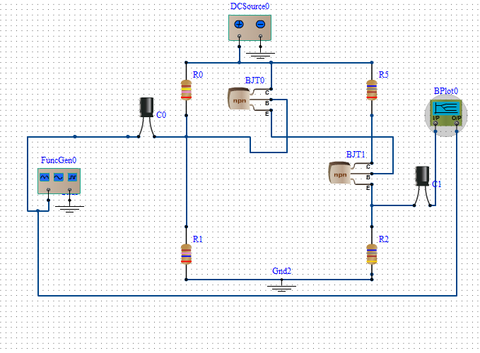
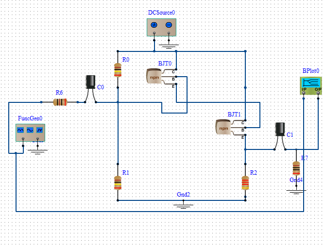
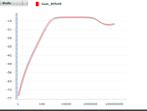
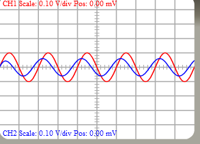
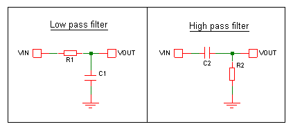
how to design the circuit,m not getting the frequency response ,,i think there is something wrong in calculation in calculation of capacitance,,however i have calculate resisistance value as R0=147 mega ohm., R5=681 OHM; R1=17.8 mega ohm;R2=680 ohm;C0= C1=10 microfarad;VCC=27 volt.
 

Re: Darlington amplifier

I think R0 and R1 are too big, and the ratio is too high. Try R0 = 100K, R1 = 33K.
The DC voltage source must be high enough. 12V to 20V is OK.
BPlot0 must be connected between C1 and ground.
 

Re: Darlington amplifier

Try to put an "AC source" instead of FunctionGeneration when doing AC analysis (Bode Plot)

And check the input/output of your BodePlotter? seems weird.. i think input should at AC source?

Hopes this is the clue~ :)
 

Re: Darlington amplifier

I think R0 and R1 are too big, and the ratio is too high. Try R0 = 100K, R1 = 33K.
The DC voltage source must be high enough. 12V to 20V is OK.
BPlot0 must be connected between C1 and ground.


I corrected the change in Bode Plot and did simulation again and I have attached the frequency response. Do u know how to design for the capacitance values for given lower and upper cut-off frequencies??

[COLOR="silver"]- - - Updated - - -[/COLOR]

yah,i got my mistake and change the connection for bode plot .can you give me the design steps for from the beginning for calculation of component..i think i m doing something wrong in calculation,i am sewnding you my calculation,please check it..

Let Vcc = 27 Volt.; β1= β2=110.(Transistor-BC 547 BP)
Let,Rs=100 Ω and Rl = 1.6 Ω
Selection of Operating point (Icq,Vcq).
Let, Icq=2.00 Ma. And Vcq=6.83 Volt.
Calculate base current;Ibq=Icq/β1. β2 =Icq/ βd ; here, βd = β1.β2
Ibq =(0.002/110*1Ω10)=0.002/12100=0.165μA.
Calculation of Rb by using K.V.L ; (Vcc –Vbe-IbRb - Ibβd .RE) =0
Ib= ( Vcc –Vbe ) /Rb + βd .RE =(27-1.5)/ (Rb+12100*680)
Rb +12100*680=25.5/0.165*10-6
Rb+8228000=(25.5*10+6 )/0.165 ;
on solving,we get Rb=146.27 M Ω

Again,Vcc-IcRc-Veb1-Ib1.Rb=0
Vcc- β1. β2Ib1Rc-Veb1-Ib1.Rb=0
Ib1 = ( Vcc –Vbe1 ) /Rb + β1. β2Rc
0.165*10-6=(27-1.5)/146.2 MΩ+12100 Rc
On calculating we get Rc = 683.4 Ω
Vb =R2*Vcc/(R+R2)
R2*Vcc = Vb (R1+R2); R2*Vcc =( VE +Vbe )( Rb+R2) +R2) =(IE.RE+Vbe) (R1+R2)
R2*27 ={(0.002*680)+1.5}{146.27*10+6 +R2}=(2.86 +1.5){146.27*10+6 +R2}
27 R2-2.86 R2 =418.33 * 10+6 ; R2 =17.33 M Ω

Input capacitance ,Cin=1/2* π* (Rs+Rin)*f1,
Where f1=fc1/10;fc1 is “lower cutoff frequeny.”
In this case,we assume that lowercutoff freq(fc1)=20 hz.
Let higher cutoff frequency,fc2=20khz.
Let source resistance(Rs=100 Ω)
Now,we have to calculate Rin for calculation of Cin.
Rin=RbII RcIIβ.re’
re ’ =0.025v/Ie ; 0.025v/Ic ( assume,Ie=Ic)
re’=10.63Ω ; β. re’=50*10.63=531.5 Ω

Now,Rin=240 K Ω II 2.2 K Ω II 0.5315 k ={ (240 K Ω *2.2 K Ω )/(240 K Ω + 2.2 K Ω)} II 0.5315 k Ω
Rin=(528/242.2)k Ω II 0.5315 k Ω =2.18k Ω II 0.5315 k Ω
=>>(2.18*0.5315)/(2.18+ 0.5315)=1.158/2.7115
Rin=0.427k Ω=427 Ω
Since,fc1=20 hz,hence f1=20HZ/10=2hz
Cin={1/2 π(Rs +Rin)*f1}={1/2*3.14*(100+427)*2}
Cin =(1/6.28*537*2) =(1/6744.72)=148.2 μ f.
Now We shall calculate output capacitance.
Cout={1/2π *(Rout+load resistance)*Fz}
Now,we shall calculate value of Cin

Let, load resistance=1.58 k Ω.
Rout=RoIIRc
Here,Ro={(Va+Vceq)/Icq}=(80+6.83)/0.00235=36.94 kΩ.
Where, V.a=Early voltage;Vceqand Icq are Operating point.
Now ,We have to calculate parameter Fz for finding Cout:
Fz=1/2 π*RE*Ce
For finding Fz,we have to calculate,Ce and for calculate Ce ,we have to find Re; So,first We will calculate, Re
Let emitter leg resistance (RE=680Ω)
We have to calculate Re; we will use formula,Re=REII{(Rs II Rb II Rc)/β )+re’}
Re=680II {(100 II 240000 II 2200)/ 50 }+10.63=680 II {(98.958 II 2200)/50+10.63}

Re=680 {(95.655/50)+10.63} = 680II {1.913+10.63} = 680 II 12.54 = 8527.2/692.54 = 12.31 Ω
Ce=1/2π*Re*fc1=(1/2*3.14*12.31*20hz)=1/1546.136=646.78 μ f.
Ce=646.78 μ f
Now we we will calculate,Fz
Fz=1/2π*RE*Ce= 1/2*3.14* 680*0.00064678 = 1/2.762= 0.362 hz

Cout=1/2 π* (Rout+load resistance)*Fz
Rout=RoIIRc=(36.94kΩ II 2.2kΩ)
Rout=(36.94*2.2)/(36.94+2.2)=81.26/39.14
Rout=2.076 kΩ=2076 Ω
Cout=1/2*3.14*(2076 Ω+1580 Ω)*0.362
Cout=1/8311.40=120.31 μf.
 

Re: Darlington amplifier

the frequency response seems like a low pass response.. should not happened if following the 1st picture at 1st post, unless u changed the arrangement of the capacitor.

in order to get a lower and upper cutoff freq. u need to design a bandpass(a zero comes 1st before the pole)

i can easily by adding a series Rx and series Cx, follow by coupling(shunt) Ry with series with Cy after the output..
then u control the Cx,Rx,Ry,Cy value and magic will happen! :p
 

Re: Darlington amplifier

i am sewnding you my calculation,please check it..
Yikes! I think you might have got lost in the maths there. I certainly got lost trying to follow it.

Here's how I'd think about it, starting with some basics:
  1. If you just want to use the circuit as an emitter follower then you don't need R5 (the collector resistor). It just gets in the way.
  2. To get the maximum voltage swing on the output, it should be biased to about half the supply voltage, so R0 and R1 can be the same value. That will result in about 12V between the emitter of BJT0 and ground, and about 15V across BJT0.
  3. A BC547 can't dissipate much power or conduct high currents. If BJT0 conducts 10mA of current, it's power dissipation will be 15V * 10mA = 150mW. That should be OK, but a bit less would be safer.
  4. We need to choose R2 to set the current through BJT0. If R2 = 4.7K, I = 12V / 4.7K = 2.55mA. That would be OK, but we can go higher too. If we reduce R2 to 2.2K then I = 12V / 2.2K = 5.45mA That should be fine. Power dissipation in BJT0 = 15V * 5.45mA = 82mW.
  5. You said β1= β2=110, so the base current of BJT0 = 5.45mA / 110 = about 50uA.
  6. Now there's a trick. A BC547's gain and speed get much worse at very low (and high) collector currents. If we want BJT1 to perform really well, it should have more than 50uA of current flowing through it. 500uA would be much better. We can fix that by adding a 27K resistor from BJT1's emitter to ground. Now there will be about 510uA flowing through BJT1. About 50uA goes into BJT0's base and 460uA goes into the resistor.
  7. BJT1's base current = 510uA / 110 = about 5uA. We don't want that current to pull the base of BJT1 more than about 0.5V below half the supply voltage, so the parallel combination of R0 and R1 should not be more than 0.5V / 5uA = 100K. So we want R1 = R0 = less than 200K. We can make R0 = R1 = 100K. The parallel combination of R0 and R1 is then 50K.
  8. Now what about frequency response? There is a low frequency rolloff at the input due to C0 and the input resistance of the amplifier, which is almost exactly equal to the parallel combination of R0 and R1 (i.e. 50K).
    The frequency is given by: F = 1 / (2*Pi*R*C)
    e.g. If C0 = 1uF, then F = 3Hz.
  9. At the output there is another low frequency rolloff due to C1 and the load resistor. The same formula applies. e.g. If C1 = 10uF and the load is 10K, then the rolloff is at 1.6Hz. If C1 = 10uF and the load is reduced to 1K, then the rolloff will be at 16Hz.
  10. You mentioned a load of 1.6 Ohms, but that isn't really practical with this circuit because the current available is so low.

Hope some of that helps.
 

Re: Darlington amplifier

yah ,i have done all these suggested by you,still not getting output,will you please suggest me values for RX,CX,RY,CY....

- - - Updated - - -

yah ,i have done all these suggested by you,still not getting output,will you please suggest me values for RX,CX,RY,CY....

- - - Updated - - -


- - - Updated - - -


- - - Updated - - -


- - - Updated - - -

yah have given R6=1 OHM;C0=I MICROFARAD;CI=10 MICROFARAD;R7=10 0HM
 

Re: Darlington amplifier

yah ,i have done all these suggested by you,still not getting output,will you please suggest me values for RX,CX,RY,CY....
What output do you want?
The output you got is correct for the values you chose.
 

Re: Darlington amplifier

I want to design this amplifier such that i get a frequency response from 20 Hz to 20kHz like a band pass filter. How should i decide it then?

- - - Updated - - -

okay, i am getting the output in time domain as well as in frequency domain ,with voltage gain nearly equal to 1,After some modifacation in the circuit .I am looking for amplification in frequency range 20 hz-20 khz,can you suggest me component values for this frequency response.
i have selected load rseistance as 2.05 kiloohm,and C1=0.5MICROFARD.can you suggest me design steps or any link which will help me for the same..

- - - Updated - - -


- - - Updated - - -

88_1339062980.png


- - - Updated - - -

100_1339063161.png
 

Re: Darlington amplifier

C0 = 220nF
C1 = 10uF
R6 = 10K
R7 = 1.2K

Add a 1nF capacitor between the base of BJT0 and ground.
 

Re: Darlington amplifier

now ia m getting the output,,will you tell me,how u come to know about 1 nf capacitor between bjt0 base and ground..will yuu give me your concepts ,how you calculate all these values..
 

Re: Darlington amplifier

how u come to know about 1 nf capacitor between bjt0 base and ground..will yuu give me your concepts ,how you calculate all these values..
For both kinds of filter, F = 1 / (2*Pi*R*C)

 
Status
Not open for further replies.

Part and Inventory Search

Welcome to EDABoard.com

Sponsor

Back
Top