Continue to Site

Welcome to EDAboard.com

Welcome to our site! EDAboard.com is an international Electronics Discussion Forum focused on EDA software, circuits, schematics, books, theory, papers, asic, pld, 8051, DSP, Network, RF, Analog Design, PCB, Service Manuals... and a whole lot more! To participate you need to register. Registration is free. Click here to register now.

How to deal with/avoid the noises on the clock signal caused by the voltage ripple in the power supply?

Status
Not open for further replies.

juliewxh

Newbie
Joined
Aug 23, 2022
Messages
4
Helped
0
Reputation
0
Reaction score
0
Trophy points
1
Activity points
58
Hello everyone,
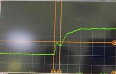
I encountered an issue that the clock signal got some noises on its edges during the transition (as is shown in the picture).
Capture.JPG

It seems it's because the power supply has some ripples caused by the digital circuit's instantaneous power. The noises are big enough to make the flip-flops toggle like there are true clock edges.
Which will be a good way to deal with this condition? Filtering the noise on the clock using a digital circuit, suppressing the noise using a capacitance, applying some strategies to enhance the stability of the power, or are there any general approaches to solve this issue?
Any suggestion will be appreciated.
Thank you very much!
 
Last edited:

Hi,

use proper decoupling on power supplies.
with a bulk capacitor as well as fast ceramics capacitors. Best: one capacitor for every power pin of every IC.

Klaus
 
you have not shown the correlation mentioned or supposed.

proper power supply filtering and bypassong on all IC's is a good idea nonetheless.
 
I doubt this is power supply ripple induced (unless you count things like simultaneous output switching sucking all the juice out of the close-in HF decoupling). Which is not ripple.

To me it looks.more like an unmatched or poorly matched transmission line. You might want to look at it from that perspective especially if the line is electrically longer than the signal edge time.

This could also be aggravated by (say) putting a spec timing measurement load on every bang-bang digital output thus adding gross displacement current sink pulse to the I/O supply rail. That is an adder to on-chip switching current. Be sure you are not causing an unrealistic application condition by mixing parametric tests (w/ burdens) with your functional testing or at least use more realistic loading.
 
Also, could you please show measurement set up....eg, did you use scope probe with long dangling ground clip, which will always make your artefact look worse.
 
Thanks all for replying, I really appreciate everyone's help(y).

We do have a decoupling capacitor on the power rail and here's the result of the simulation when applying the instantaneous power:
1661460819033.png


It seems not like the issue of the power rail then. We suspect the noises on the clock signal are caused by the noises on the ground rails, otherwise, it could have something related to the fanout of the clock pin.

@cupoftea
Here's the picture of the noise on the clock signal with measurement:
1661461682785.png

I'm still wondering if there is a general way to deal with the noises on the digital clock signal if it exists anyway after all tries.
 

Again, the "whoop-de-do" at half-transition is a
hallmark of impedance mismatch, try lifting the
pin (if practical) and reconnect through some
different resistor values to see how the edge-shape
changes.
 

Attachments

  • AN246.pdf
    216.8 KB · Views: 112
  • NationalAN108.pdf
    251 KB · Views: 105
  • transmissionline.pdf
    98 KB · Views: 103
Hi,

off tpoic hint:
Every PC / every OS provides a "screenshot feature". Upload a screenshot as .PNG to get best quality with low filesize.

A photo of a PC monitor results in worse qulity with bigger files. If a photo is used: switch off the flash and upload it as .JPG. (maybe with 1024 pixel in width and 35% jpg quality)

****
After reading the headline, I assumed you already determined the root cause was the power supply.
But now I´m not sure about this.
Please tell us what is "expectation" and what is "truth".

It seems you have a schematic, maybe even a PCB layout. If so, then please show both.

Klaus
 
If you want textbook-looking clock waveforms do the following;

1. Decouple IC with 10nF to 100nF across Vdd:Vss pins.
2. Due to trace inductance and capacitance to ground plane the CMOS driver Ron (=Zol+Vol/Iol) must be matched to your load whenever the load rise time is as fast or faster than the prop. delay. due to path length by adding a small resistance. But not too much so that voltage margin is lost, so there is a tradeoff.
3. Your characteristic impedance Z(f)=sqrt(L/C) when matched will give perfect reflection-free edges but only 50% of the voltage. So the trick is to minimize the path length , and add a small R in the range of 20 to 33 ohms.
4. Use a 10:1 probe calibrated with a very short probe ground or removed using only the pin and coaxial barrel between two short pins near the IC for signal and gnd using resistor wire or equiv.
 
we don't know where the clock signal is being measured ....!

at the output of the clock generator ... ?

down a long transmission line next to a non matched termination ... ?

there is no way to answer the question usefully - as scant information is supplied - a detailed pic of the pcb taken from the creation pcb program would be best here .... with the relevant track highlighted ...
 
@Easy peasy
We put the clock signal from the clock generator to the clock pin inside the chip by sticking a probe to that pin, then measured the wave on the connecting wire.

@D.A.(Tony)Stewart
Thanks for the suggestions, I will forward them to our analog engineer to see if we can do something.

@KlausST
Thank you for the information.
The "expectation" is that there are no noises big enough to make the flip-flops toggle.
The "truth" is that some of the noises are big enough to make the flip-flops toggle, which results in the malfunction of a certain percentage of our chips. (According to the liberty timing files of the foundry, a noise of 0.2 ns wide and 1.0 V high can make a flip-flop toggle.)
So I'm wondering if there's a general way to filter the noises on the clock signal (either digital method or analog method).
 

Again, the "whoop-de-do" at half-transition is a
hallmark of impedance mismatch, try lifting the
pin (if practical) and reconnect through some
different resistor values to see how the edge-shape
changes.
Thank you so much for the suggestion and the documents. I'll study them and discuss them with our analog engineer.
 

you need a very short gnd connection too - i.e. just 10mm or less, not a long wire with a croc clip to some gnd point miles away ...
 

The "truth" is that some of the noises are big enough to make the flip-flops toggle, which results in the malfunction of a certain percentage of our chips. (According to the liberty timing files of the foundry, a noise of 0.2 ns wide and 1.0 V high can make a flip-flop toggle.)
So I'm wondering if there's a general way to filter the noises on the clock signal (either digital method or analog method).
....Thanks, it sounds like you dont have any particular cct in mind, but that you work in a foundry producing these chips, and you want to see if they are false clocking.(?)

As such, there will be definite highly "noise busting" Test jigs for this purpose...they will be highly standardised, and the managers of your foundry will know all about them.....it sounds like they are kind of testing you out, to see how much you can get into this?....before they show you the actual way they test for this
 

If you know how to control impedance of wires, traces, choice of cables then you can avoid reflection ringing by matching impedance with a chosen series resistor. Remember 3.6V logic is around 25 ohms and traces tend to be higher.
 

Status
Not open for further replies.

Similar threads

Part and Inventory Search

Welcome to EDABoard.com

Sponsor

Back
Top