Rajashri.Shevale
Junior Member level 2

create PDF of actual size in altium which shows pads and path on bottom layer
hello
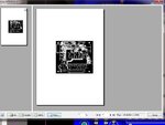
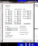
i have created a pcb on altium 10. now i want to make it as a pdf of actual physical size of components and all , so that i can make an actual board. i am not getting how to create pdf in altium .
plz help me
hello
i have created a pcb on altium 10. now i want to make it as a pdf of actual physical size of components and all , so that i can make an actual board. i am not getting how to create pdf in altium .
plz help me