Continue to Site

Welcome to EDAboard.com

Welcome to our site! EDAboard.com is an international Electronics Discussion Forum focused on EDA software, circuits, schematics, books, theory, papers, asic, pld, 8051, DSP, Network, RF, Analog Design, PCB, Service Manuals... and a whole lot more! To participate you need to register. Registration is free. Click here to register now.

How to connect CMOS Body( Bulk) connection of several mosfets in layout

Status
Not open for further replies.

Ali263

Member level 1
Joined
Aug 21, 2020
Messages
40
Helped
0
Reputation
0
Reaction score
1
Trophy points
6
Activity points
450
I have to to layout of 2 stage amplifer in cadence 65nm. For reference i am given a design in which i am feeling difficulty. In layout all mosfet bodytie_type is left to none.
I was wondering how can the bulk be connected to gnd or vdd if all bodytie_type is selected to be none?

Secondly, if we are having9 mosfets in a design do we have to connect bulk of every mosfet separately to gnd or vdd?

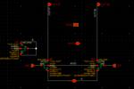
In picture you can see the main differential and dummy mosfet pair where bulk is grounded but in layout bodytie_type is none?
 

Attachments

  • t.PNG
    t.PNG
    14.9 KB · Views: 363
  • vrg.PNG
    vrg.PNG
    53.4 KB · Views: 341

The bulk connection is not the easiest thing to do in layout. You have to connect a certain layout (depends on technology). It might be ptap or ntap very close to the pwell of each nmos transistor. You have to ask a senior or someone who uses the technology to show you an example of connecting bulk of a single transistor then you can follow the procedure in all transistors.
 

Is your AVSS the substrate's voltage ? If that's the case, create a guard ring around your diff pair including the dummies. It's quite rare where you use the mosfet's default guardrings due to area constraints. Because if you open the guard ring options, it will bring bulk connection on each individual transistor which is cause your layout area to be bigger. Therefore you don't need to connect each transistor separately. Guard ring around the whole structure is sufficient enough. If you want to better connection and less resistance you can increase number of contacts of the guard ring but it can also increase noise on substrate. It's little bit trade-off as always.
 
Status
Not open for further replies.

Part and Inventory Search

Welcome to EDABoard.com

Sponsor

Back
Top