Continue to Site

Welcome to EDAboard.com

Welcome to our site! EDAboard.com is an international Electronics Discussion Forum focused on EDA software, circuits, schematics, books, theory, papers, asic, pld, 8051, DSP, Network, RF, Analog Design, PCB, Service Manuals... and a whole lot more! To participate you need to register. Registration is free. Click here to register now.

how to connect and interface with this switch?

Status
Not open for further replies.

Antenna (^.^)

Member level 3
Joined
Jul 6, 2015
Messages
54
Helped
0
Reputation
0
Reaction score
0
Trophy points
6
Activity points
499
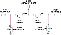
I don't understand how to connect and interface to this switch, AS214-92LF
I've read the data sheet but it didn't help me.

V1 and V2 correspond to the control voltage and I think vcc but which is which?
J1, J2, J3 truth table what does isolation and insertion loss state mean? where is on/off?

Are the control voltages to choose between J1,J2,J3 digital or analogue?

What is the impedance of it? is it 50 ohms?
 

HI

J1,J2 and J3 are analog in/out put, V1 and V2 and selection controller pin, Isolation means there is no connection and Insersion loss means there is connection with some loss in output. V1 and V2 are logic voltage(2.7V-5V)

Thanks,
 

Oh, okay so both v1 and v2 are respond to digital logic input voltage from 2.7V to 5V for high (on). The J1, J2, J3 output a voltage that is analogue. But there is no Vcc for this switch?

- - - Updated - - -

Could you please explain further what you mean by stripline?
 

correct no Vdd ( or Vcc) as these are GaAs Series pass switches.
9908_Figure3x250.gif


If this doesn't make sense, using this part may be beyond your bandwidth at the moment.

Since the part is AC coupled, internal biasing may be done . This is just a simplified diagram.

Stripline is a form of controlled impedance defined by a transmission line property of distributed inductance and capacitance such that the impedance is constant for RF up until the dielectric properties change. For example when the PCB track width is equal to it's depth of dielectric for e~4 it turns out to be near 50 Ohms, which is used for this part. Although for Teflon the e is different, and track width will be different for 50 Ohms.
 

so stripline is a transmission line used to feed the signal to and from the switch, similar to a coplanar waveguide or microstrip transmission line?
And the impedance will be constant (not changing) and relate to the stripline dimensions required for 50ohm impedance?
 

I suggest to read this Skyworks application notes to get some insight about GaAs switch operation https://www.skyworksinc.com/uploads/documents/200363A.pdf

GaAs RF switches are depletion mode NJFETs. They are normally on and can be brought to high impedance by a negative gate voltage relative to source and drain. The schematic in post #5 shows PJFETs and has to be respectively corrected. Also AS214-92LF doesn't involve any switches to ground, it's a double-throw switch.

Positive control voltage operation of GaAs switches uses a trick by AC coupling the signal path. Source and drain are automatically biased to a positive voltage because one of the control inputs is regularly high.

If you want to operate the switch in a non-standard configuration which includes a state with both FETs off, you must provide a separate bias path. GaAs switches have an oustanding low Rdson*Cswitch number, so it can be interesting to use them for other applications than RF switching. Understanding their operation is required in this case.

Although 50 ohm matching is the usual situation, the switches aren't restricted to it.

What's your application?
 

It is part of a frequency reconfigurable patch antenna implemented on a pcb.
There are five adjacent patches (large areas of pcb copper). Not all of the patches are turned on, it depends on the frequency the user selects.
For example if the user chooses a frequency of 2.1GHz, only the first two patches will be active. If the user chooses a frequency of 1.8GHz only the first three patches
will be active.

The application of the switch is that is connected between each of the five patches, and a microcontroller will let the rf signal through (on) or block it (off) depending on
which frequency selected (and hence which patches are supposed to be on).
 

Yes , with Depletion Mode GaAs FETs the switch is closed with 0V.
V1 closes J2 and
V2 closes J3 so both should never be closed or open at same time as indicated in spec.as invalid.
So that exclusive switch enabled by one or other is used with Vx=0V.
 

Yes , with Depletion Mode GaAs FETs the switch is closed with 0V.
V1 closes J2 and
V2 closes J3 so both should never be closed or open at same time as indicated in spec.as invalid.
So that exclusive switch enabled by one or other is used with Vx=0V.
The dataheet table shows the states used with standard SPDT operation. Other switch states (e.g. both switches off) are possible though with respective bias circuit.
 

The dataheet table shows the states used with standard SPDT operation. Other switch states (e.g. both switches off) are possible though with respective bias circuit.

If the switched port is terminated, then switching as a SPST will create 0dB return loss if unterminated.
Spec indicates All other conditions not recommended.

Preferred operation might be to terminate the unused port being a dummy load to avoid S12 reverse coupling and S11 poor return loss, thus using the SPDT function.
 

Status
Not open for further replies.

Part and Inventory Search

Welcome to EDABoard.com

Sponsor

Back
Top