Continue to Site

Welcome to EDAboard.com

Welcome to our site! EDAboard.com is an international Electronics Discussion Forum focused on EDA software, circuits, schematics, books, theory, papers, asic, pld, 8051, DSP, Network, RF, Analog Design, PCB, Service Manuals... and a whole lot more! To participate you need to register. Registration is free. Click here to register now.

How this circuit works?

Status
Not open for further replies.

muhammad11

Member level 2
Joined
Nov 1, 2013
Messages
43
Helped
0
Reputation
0
Reaction score
0
Trophy points
1,286
Activity points
1,572
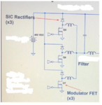
Kindly explain the working of this circuit especially when FETs are switched on / Off and the function of Sic diode here?
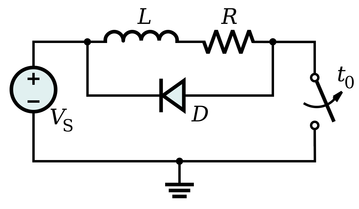
Q 1. How the circuit works when FET is turned on/off?

Q 2. What are purpose of SIC Diodes?

Q.3 What is the function of Inductor?

Q.4 What is the name and functionality of this circuit
(circuit attached)
 

Kindly explain how we are supposed to explain an invisible circuit.
 

Kindly explain how we are supposed to explain an invisible circuit.

In this circuit when FET is turned on its mean drain is shorted to ground (0 volt).But i donot know what will be the purpose of Sic
diode

(circuit attached)
 

Attachments

  • how it work.png
    how it work.png
    622.6 KB · Views: 129
Last edited by a moderator:

In the shown circuit, current and energy flow is only possible into the inductor from the right side. To understand how it works, we should know what's connected there.

At first sight, the circuit looks like a multi-phase boost converter.
 

    d123

    Points: 2
    Helpful Answer Positive Rating
Thanks for your reply.. At the right side of the circuit there is amplifier stage. Kindly now explain how amplifier stage is supplying current or energy to inductor. I am attaching more detail circuit kindly explain the working of the circuit.
Regards

1.png
 
Last edited by a moderator:

what you call an “amplifier” looks to me like a box with the letters F E T in it. Regardless, the current in the inductors does not come from the amplifier, it comes from the power Supply by the charging and discharging of the cap and inductors.
 

what you call an “amplifier” looks to me like a box with the letters F E T in it. Regardless, the current in the inductors does not come from the amplifier, it comes from the power Supply by the charging and discharging of the cap and inductors.
yes in amplifier stage there are FETs in that circuit. Can you explain the working of SIC diode in the circuit?
 

the diode clamps the inductive flyback voltage when an FET turns off.
 

the diode clamps the inductive flyback voltage when an FET turns off.
Sir kindly explain the circuitry in detail and in simple way.When transistors(Q5/ Q6/ Q7) are turned on its mean 0 volt (ground volt )at inductor L1 and Sic diode. kindly explain the working of the circuit.
 
Last edited:

There's not consistent circuit schematic yet that can be explained. The connection of "amplifier# FETs isn't clear. If 400V is the power supply, where's the circuit output, what's the load.
 

There's not consistent circuit schematic yet that can be explained. The connection of "amplifier# FETs isn't clear. If 400V is the power supply, where's the circuit output, what's the load.
Sir The complete circuit is attach herewith..kindly explain the working of whole circuit..


Regards
 

Attachments

  • circuit complete.jpg
    788.4 KB · Views: 107

Thanks, now the circuit makes sense. The left part is a three phase buck converter, reducing 400 V input to 0 - 400 V fed to the full bridge on the right. Unlike the typical buck converter with common negative ground this circuit has common positive node and respectively position of transistor and diode flipped.
 

An explanation of flyback diodes used to clamp HV transients from inductive
loads.


w/o diode (large transient at switch) -

1617536826534.png


with diode -

1617536702846.png


Regards, Dana.
 

Attachments

  • 1617536282688.png
    1617536282688.png
    69 KB · Views: 86
Last edited:

The reference to fly-back clamp misses the point. Clamping is a side effect, the circuit purpose is voltage down conversion.
 

Thanks, now the circuit makes sense. The left part is a three phase buck converter, reducing 400 V input to 0 - 400 V fed to the full bridge on the right. Unlike the typical buck converter with common negative ground this circuit has common positive node and respectively position of transistor and diode flipped.
Kindly explain the whole circuit working. For example when FET is closed mean 0 volt on drain then how inductor will store energy etc. AS dc is applied then sic diode is reversed biased and capacitor will act as open circuit due to DC supply (400 v). Then how first stage step down and provide 0 to 400 volt variable DC?
--- Updated ---

The reference to fly-back clamp misses the point. Clamping is a side effect, the circuit purpose is voltage down conversion.
Kindly explain the working of the circuit especially the first section of the circuit
 

You’re awfully demanding. We have explained the purpose of the diodes, as you asked. Fvm has explained the basic function of the circuit. Danadakk has actually gone to the trouble of simulating the inductive flyback for you.

Maybe it’s time for you to read a book or do some research of your own, instead of insisting we do a complete circuit analysis for you.
 
The converter topology is (multi-phase) buck converter. As for the basic theory of operation and waveforms, you can refer to this link. https://en.wikipedia.org/wiki/Buck_converter#Concept

Polarity is however flipped in your circuit, as shown in the below schematic

1617611170465.png
 
Last edited:

You’re awfully demanding. We have explained the purpose of the diodes, as you asked. Fvm has explained the basic function of the circuit. Danadakk has actually gone to the trouble of simulating the inductive flyback for you.

Maybe it’s time for you to read a book or do some research of your own, instead of insisting we do a complete circuit analysis for you.
It is forum for all to share the technical problems. If someone is not genius like you then please let him to ask again and again so that concept may be cleared to him. Hope you will understand my point.
--- Updated ---

The converter topology is (multi-phase) buck converter. As for the basic theory of operation and waveforms, you can refer to this link. https://en.wikipedia.org/wiki/Buck_converter#Concept

Polarity is however flipped in your circuit, as shown in the below schematic

View attachment 168598
Thank you Sir, the main confusion in my circuit was the polarity of diode which compel me to ask the functionality of the circuit. anyways thank you
 

Status
Not open for further replies.

Similar threads

Part and Inventory Search

Welcome to EDABoard.com

Sponsor

Back
Top