Continue to Site

Welcome to EDAboard.com

Welcome to our site! EDAboard.com is an international Electronics Discussion Forum focused on EDA software, circuits, schematics, books, theory, papers, asic, pld, 8051, DSP, Network, RF, Analog Design, PCB, Service Manuals... and a whole lot more! To participate you need to register. Registration is free. Click here to register now.

Working of this circuit

FreshmanNewbie

Full Member level 6
Joined
May 10, 2020
Messages
386
Helped
0
Reputation
0
Reaction score
2
Trophy points
18
Activity points
3,857
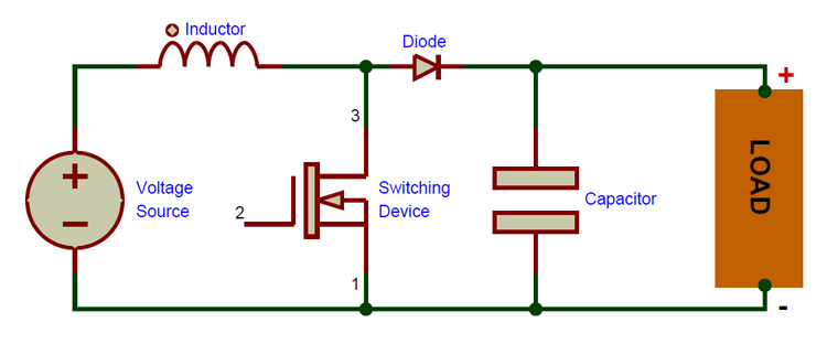
I've got this simulation circuit below.

This IC is a boost converter. I am curious to understand how the input is stepped down using a boost converter.
Can someone explain the working and the graph too?
Why is there a flat line at -6V?

enter image description here
 
The IC has its own boost converter built in, so it can bias its internal high-side transistor. (This seems to be described in the data sheet.) An N-device in that function requires sufficiently high bias voltage to turn it fully On. The bias voltage needs to be greater than the power supply.

I believe the IC's output pin provides pulses of positive polarity at supply voltage. The output stage is configured as a buck boost converter.
 
Hi,

sorry but I do not get your point, the MCCP16301 is clearly advertised as a buck/step-down converter and not as a boost converter. Further, your attached schematic doesn't follow the typical application shown in the datasheet at all. Have a look on the circuitry on pate 2 in the datasheet. Check the GND connection of your circuitry and how it is connected to the IC, as your attached Vout plot is measured with respect to GND.

BR
 

LaTeX Commands Quick-Menu:

Similar threads

Part and Inventory Search

Welcome to EDABoard.com

Sponsor

Back
Top