hiramlee
Junior Member level 1
- Joined
- May 15, 2012
- Messages
- 16
- Helped
- 0
- Reputation
- 0
- Reaction score
- 0
- Trophy points
- 1,281
- Location
- Chengdu,China
- Activity points
- 1,408
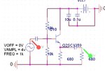
I design a very simply transistor circuit, and we all know about it.
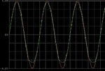
The frequency of input signal is 1KHZ ,and magtitude is 1Vp-p.when the load resistor Rl5=100K, the Pspice give me such a result as below:
在输入为1KHZ,1Vp-p情况下,在100KHZ负载情况下该电路的仿真效果图:
**broken link removed**
Obviously ,the output wave was cut off when greater than 0.6V, and Magnification didn't exactly equal to 5 as we want.
可见输出在正0.6V左右出现了截止情况,大于为0.67V的输出被削峰。而且负的最大输出为2.1V放大倍数没有达到预想的5倍。
**broken link removed**
这是为什么么呢?
Now i change the R19 to 10K ,and it became:
下面随意改动几个数据,将VCC串联电阻减小到10K的输出:
**broken link removed**
Then, we cancel the R19,and now it's better.and I want to know why.
削峰现象消失,此时输出最大值为2.25,基本达到预期目标。
把R19减小为0时,情况又有好转。
请问这是什么原因呢
- - - Updated - - -
I guess that maybe the R19 lead to a improper DC operating point and that's my wrongdoing.
Vo=Vcc-Ic*Rc and approximate: Vcc-Ie*Rc,=Vcc-(Vb-Vbe)/Re*Rc,
when i set a improper Dc operating point , Saturated distortion occured
And if Vb is too low, a little Vi lead to Saturated distortion
And if Vb is too high, a big vi lead to Saturated distortion
Is it true and anyone can tell me something about it .
many thanks.
- - - Updated - - -
Someone tell us that it's better set Vc to half of VCC.

