Welcome to our site! EDAboard.com is an international Electronics Discussion Forum focused on EDA software, circuits, schematics, books, theory, papers, asic, pld, 8051, DSP, Network, RF, Analog Design, PCB, Service Manuals... and a whole lot more! To participate you need to register. Registration is free. Click here to register now.
You have the solution so it is difficult to know what to add, other than words to replace equations. Have you a specific bit of the description which doesn't make sense?
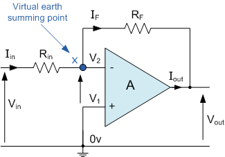
Maybe M1 is confusing? It is a 'grounded gate' amplifier, although the gate is connected to a fixed bias point rather than actual ground. With the gate fixed, the input is the source and the output is the drain. When the source voltage goes down it turns the transistor on harder, making the drain voltage also go down.
It might look simpler if you remove Iin and Rf and joined point P to the source of M1. The feedback mechanism will be similar but with fewer parts to cause confusion.
This site uses cookies to help personalise content, tailor your experience and to keep you logged in if you register.
By continuing to use this site, you are consenting to our use of cookies.