Continue to Site

Welcome to EDAboard.com

Welcome to our site! EDAboard.com is an international Electronics Discussion Forum focused on EDA software, circuits, schematics, books, theory, papers, asic, pld, 8051, DSP, Network, RF, Analog Design, PCB, Service Manuals... and a whole lot more! To participate you need to register. Registration is free. Click here to register now.

How does IR2110's HIGH-SIDE Internal Circuity work ?

Status
Not open for further replies.
Hi Gary
If you use a mosfet that has an internally diode , it can handle your aim as well . i.e if your mosfet has not any internally diode , you can connect it externally !
I'm a bit confused that what you want to do exactly . because you talked about SG3526 . it is a complete driver ! are you trying an SMPS ?
Best Wishes
Goldsmith
 
Hi goldsmith,

please see attached schematics.
the SG3525A feeds the opto-coupler and then the driver/buck.
the buck design schematic isnt updated so never mind that (i will place another hexfet).

yes this is a generic SMPS- buck converter

btw - why do we need the diode between source and drain.

i've read the two papers you wrote. great explanation but i dindt understand how any of the diode in parallel the mosfets will conduct when they are in reveresed bias.
 

Attachments

  • POT_SET_0.5_CT_PWMoutput.pdf
    51.3 KB · Views: 78
  • POT_SET_ALL_OptoInput_DriveCircuit.pdf
    69 KB · Views: 84

Humm , SG3525 is a good choice for your aim because it can create enough dead time as well .
What is your problem now ?
A question , why you connected those out puts together with two diodes ?
 

another quesion please: the bootstrap drive process should happen only once on the start-up of the circuit. correct? in steady-state the capacitor will always be full of charge ?
 

Of course . it is correct .
And another thing that can be interesting for you is , a transformer driver . ( but it's quality isn't as high as a mosfet driver .)
 
okay. so the "wrong" buck configuration was correct only for steady-sate period of time. not for the initial time. i understand.

so anyways, how do i connect the LIN ? is it ok to leave it grounded in the IR2110 ?

the only modification i need to do is connect the other hexfet to the LOW SIDE output of the driver.

i wonder how the buck configuration will be then. can you draw a sketch ? according to my buck schematics ?

The two switch topology suggested by goldsmith is a synchronous buck configuration. It requires to drive the low side switch with a complementary signal, with sufficient dead time between low and high side drive signals. In so far LIN has to be connected.

I personally dislike the idea of a driver circuit dictating the output configuration. It's O.K. if you want a synchronous buck for performance reasons, otherwise i would rather think of a different driver option.
 

Humm , SG3525 is a good choice for your aim because it can create enough dead time as well .
What is your problem now ?
A question , why you connected those out puts together with two diodes ?

i tie the two outputs (output A and output B) because each output produce only 1/2 cycle. Output B is 180 degree phase shifted from Output A.
when you use these two outputs independently, you get two seperated outputs with 180 degree phase difference and only 1/2 cycle. Output A will result first 1/2 cycle and output B will result the latter 1/2 cycle. They both symmetrical. when you tie them up - you get a whole cycle.

why diodes?
because the SG3525A has a totem-pole configuration on the outputs. if you tie the outputs together without diodes, the outputs will interfere each on another because of the totem-pole configuration.

- - - Updated - - -

Of course . it is correct .
And another thing that can be interesting for you is , a transformer driver . ( but it's quality isn't as high as a mosfet driver .)

okay. so the "wrong" buck configuration was correct only for steady-sate period of time. not for the initial time. i understand.

so anyways, how do i connect the LIN ? is it ok to leave it grounded in the IR2110 ?

the only modification i need to do is connect the other hexfet to the LOW SIDE output of the driver.

i wonder how the buck configuration will be then. can you draw a sketch ? according to my buck schematics ?

thank you alot !

Gary

- - - Updated - - -

i have another question...i'll explode soon :)

you explained about LO and HO switching relationship according to LIN and HIN inputs.
does the bootstrap capacitor fully charge on the first cycle ? i.e when LO=1/HO=0 initially. and then when HO=0/LO=0 the capacitor supply drive voltage to the higher mosfet.
are there any more and more cycles of LO=1/HO=0? if not. its like a one-time switch for startup circuit. how will that be possible in reality ?
 
tie the two outputs (output A and output B) because each output produce only 1/2 cycle. Output B is 180 degree phase shifted from Output A.
when you use these two outputs independently, you get two seperated outputs with 180 degree phase difference and only 1/2 cycle. Output A will result first 1/2 cycle and output B will result the latter 1/2 cycle. They both symmetrical. when you tie them up - you get a whole cycle.

why diodes?
because the SG3525A has a totem-pole configuration on the outputs. if you tie the outputs together without diodes, the outputs will interfere each on another because of the totem-pole configuration.
Dear Gary
Thank you for that explanation , i didn't know about this action . but it still is not clear to me that how with this method we can increase the D.C . if you explain it i'll be grateful .
Let back to your problem :
okay. so the "wrong" buck configuration was correct only for steady-sate period of time. not for the initial time. i understand.

so anyways, how do i connect the LIN ? is it ok to leave it grounded in the IR2110 ?

the only modification i need to do is connect the other hexfet to the LOW SIDE output of the driver.

i wonder how the buck configuration will be then. can you draw a sketch ? according to my buck schematics ?

thank you alot !

Gary
Follow things that FvM told instead of Lin . he is quite right .
And sketch of what ? a buck with two switch ?
i have another question...i'll explode soon :)

you explained about LO and HO switching relationship according to LIN and HIN inputs.
does the bootstrap capacitor fully charge on the first cycle ? i.e when LO=1/HO=0 initially. and then when HO=0/LO=0 the capacitor supply drive voltage to the higher mosfet.
are there any more and more cycles of LO=1/HO=0? if not. its like a one-time switch for startup circuit. how will that be possible in reality ?
Don't confuse about boot strap method . at first cycle the circuit will recover itself . in practice some first cycles are not important . but if there are important for you , a simple pulse transformer can be good . but i don't think that transient time is important for you . isn't it ?
Good luck
Goldsmith
 

dear goldsmith,

it is really nice that you - mighty goldsmith can learn something from someone like me. i'll take it as a compliment :grin:

about the PWM - i may added some confusion there - the two outputs waveforms are not exactly shifted but horizontally flipped from each other. they are still 1/2 cycle each. combining them together you gain full range D.C.
hope it is clear now.
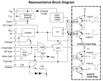
please see the representative block diagram attached here, to understand the output section better:

SG3525A Internals.PNG


about the sketch, please see my PDFs i just attached earlier. one of them shows the drive connection to the buck using asynchronous buck configuration.
how can i modify it to use two switches (synchronous buck configuration you suggested).

about the recovery time of the bootstrap capacitor. yes i understand you. correct.
what signal goes to LIN of the driver? again - see the two PDFs i attached earlier. one PDF shows the PWM (the SG3525A) and the other one is the second part schematic - the optocoupler, driver and buck.

Gary
 
Last edited:
Oh thank you according to the attached diagram now i completely understood that how with that way we can increase D.C .
Ok , tomorrow i'll write some papers about buck converters for you . i hope thus you can get the idea to complete your project as well .
Best Wishes and thank you for your clarification . ;-)
Goldsmith
 

no problem dear goldsmith !

looking forward for your tomorrow's papers.

have a good night my friend

Gary
 

btw - can you recommend any reliable app note to read about how power mosfet work in principle ?

EDIT: i'm looking for something simple and easy. not too scientific.

thank you
 
Last edited:

Dear Gary
Hi
I wrote somethings for you , but it isn't complete yet . because today i wan not in my home and i was pretty busy . but i promise you that i'll send it to you soon .
BTW : do you like SMPS , really ? if yes , can you give me your email ? if yes , if you stay just some minutes i can send you many references .
Best Wishes and sorry because of this delay .
Goldsmith
 

hi,

well its not that i love it, but i have a project to hand and just need to explore the most of it in order to make sure i make everything properly.

its okay - any help is accepted happily while you can.

Also, i need to hand the papers tomorrow so no time for more explorations :|

Gary
 

Status
Not open for further replies.

Similar threads

Part and Inventory Search

Welcome to EDABoard.com

Sponsor

Back
Top