Continue to Site
Follow along with the video below to see how to install our site as a web app on your home screen.
Note: This feature may not be available in some browsers.
ytliang said:hello,
Could someone please give me some insights on high voltage mosfets layouts and why they are drawn that way?
Thanks
mviswa said:Actually i dont know what is ment by HV mosfet ..
1. usually nowday day's all chips work at different voltages like core voltage & io voltage. usually io voltage voltages devices called TG devices , where tox more compare to core voltage transistors i.e. digital logic. TG MOSFETS will operate at more voltage than core Mosfets.
2. High voltage Mosfets also called DMOS/VDMOS transistrors. these transistor crosssection totally different from conventional mosfets to handle high voltage/high currents. In this transistors Drain extended under gate region more.
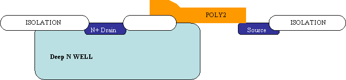
The drain extension under the gate forms a lighlt doped region between drain and channel that the high voltage can be dropped across such that there is no punchthrough or breakdown between drain and source. These kinds of transistors are good for 40V and below. For higher voltages drift regions are required.
For very high voltage MOSFETs, a thick N- epi layer is used as a drift region to drop the high voltages. Filed rings are also used to shape the depletion to keep the high field edges of the depletion zone away from critical areas. Thus, the layout of very high voltage transistors is very different from conventional CMOS.[/img]
Find here a paper about HV MOS structures.If you any other source let me know
hello,
Could someone please give me some insights on high voltage mosfets layouts and why they are drawn that way?
Thanks
Find here a paper about HV MOS structures.
@Leo: I think poly field plate doesn't generate the TOX, but is placed over it.
")