cjrathi
Member level 2
Hi,
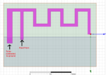
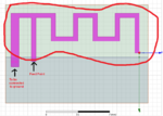
I am designing a 2.4GHz PCB antenna (F-type). Snap attached. This design is already verified at 2.4GHz, since i have seen it in one paper.
I want to design similar kind of antenna for 2.4GHz and 5Ghz band, but before starting that I want to simulate existing designed and proven antenna and verify that my HFSS set up is correct.
I have few queries:-
1. What type of excitation I should give at feed? How should I give it? Should it be vertical from substrate bottom to feed entry point? Or there is some other technique to do that?
2. How should I connect patch to ground ? Shall I put gnd plane on top as well as bottom ? How to connect top and bottom plane to each other?
3. What should be other basic settings like Solution type?
4. Shall I take patch/gnd plane as sheet and then assign it as perfect E, or I make patch as a box of small height and assign it as PEC material?
Could any body help me in this?
Thanks,
Chaitanya

