Continue to Site

Welcome to EDAboard.com

Welcome to our site! EDAboard.com is an international Electronics Discussion Forum focused on EDA software, circuits, schematics, books, theory, papers, asic, pld, 8051, DSP, Network, RF, Analog Design, PCB, Service Manuals... and a whole lot more! To participate you need to register. Registration is free. Click here to register now.

help with cmos tg dynamic shift register

Status
Not open for further replies.

andrea22

Junior Member level 2
Joined
Oct 1, 2010
Messages
21
Helped
1
Reputation
2
Reaction score
0
Trophy points
1,281
Activity points
1,427
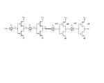
Does anyone have any tutorial about cmos tg dynamic shift register?
I need an explaination how this circuit works.
What I ment why this circuit only works with non-overlapping clocks,
or why this circuit can't work with overlapping clocks?
I need to prove why this circuit can't work with overlapping clocks.
 

Attachments

  • cmos tg dynamic shift register.JPG
    cmos tg dynamic shift register.JPG
    14.1 KB · Views: 157

Well, are you still having a trouble to understand the over-lapping and non-overlappign clock thing ???
What would happen if you feed 010101 pattern to that circuit with overlapping clock ? If you think it still works in this scenario, you probably don't fully understand synchronous circuit and need to go back to the textbook.
 

As you see this shift register is consists of 4 dynamic d latches or two d dynamic flip-flops.
With non-overlapping clocks shift register works ok.
But when I use overlapping clocks at the output of the second inverter I get smaller voltage then
Vdd (Vdd=5v,and I get 2.5v),that's what I don't understand.
I know that with overlapping clocks all TG are on at the same time,
but I don't know how to prove how that effects that this circuit can't work with overlapping clocks?
 

They are transmission gates, not pass transitors and all the node must full swing. Only possible scenario is you are using pass transistors.
 

That is happening when I use overlapping clocks,
really I get smaller voltage then
Vdd (Vdd=5v,and I get 2.5v).
When I used non-overlapping clocks everything is ok.
 

That wouldn't happen. I have designed a parity checker with multiple stages of transmission gates and it's a combinatorial circuit therefore that's exactly the same situations as overlapping clock case in your example. It worked perfect on silicon without skewing the threshold of inverters.
Your problem is either your circuit is not exactly as shown in the picture, or simulation environment.
 
Last edited:

If both transmission gates (billteral switches) can be closed at the same time that will causing mixing of old and new data and therefore loss of data integrity!
Is that right?
 

Sorry I don't know what your focus is in this discussion.

Mixing new and old data is obvious if the clock is overlapped and that's what I thought the point is in this thread, hence my post #2. Then you started saying one of the nodes are not on full swing, that leaves me thinking that voltage issue is what you are pursuing. Clear up what you mean "need to prove why this circuit can't work" part..
 

Status
Not open for further replies.

Part and Inventory Search

Welcome to EDABoard.com

Sponsor

Back
Top