Continue to Site

Welcome to EDAboard.com

Welcome to our site! EDAboard.com is an international Electronics Discussion Forum focused on EDA software, circuits, schematics, books, theory, papers, asic, pld, 8051, DSP, Network, RF, Analog Design, PCB, Service Manuals... and a whole lot more! To participate you need to register. Registration is free. Click here to register now.

Help need for drawing IIP3 and P1dB using AWR MICROWAVE OFFICE.

Status
Not open for further replies.
Dear RealAEL ,

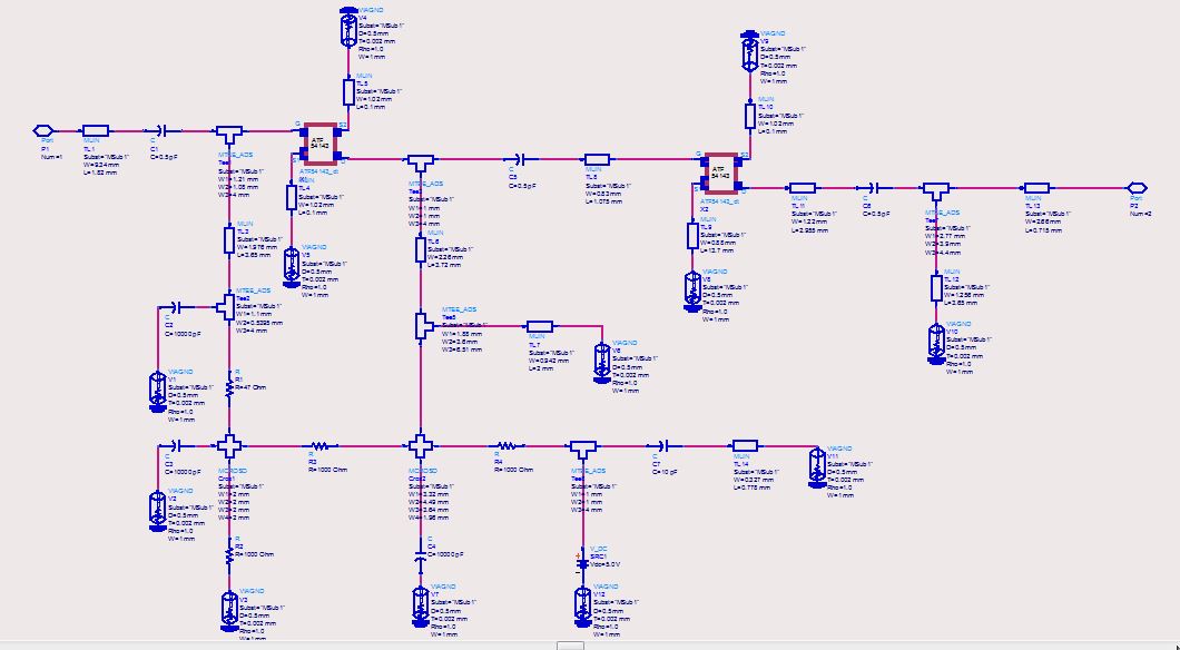
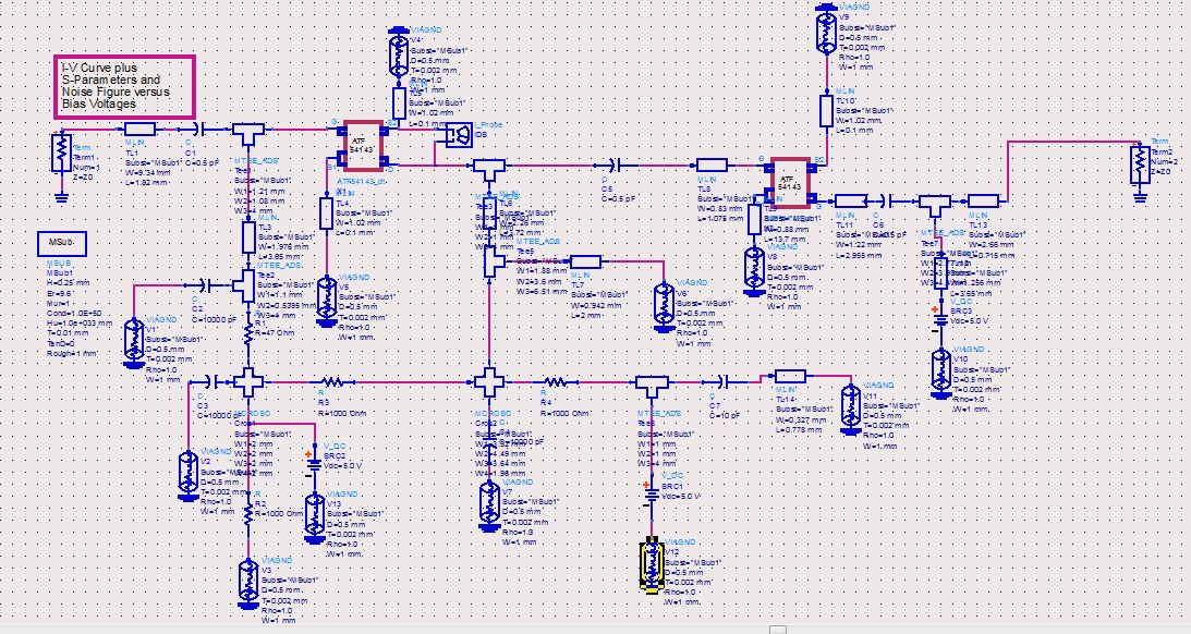
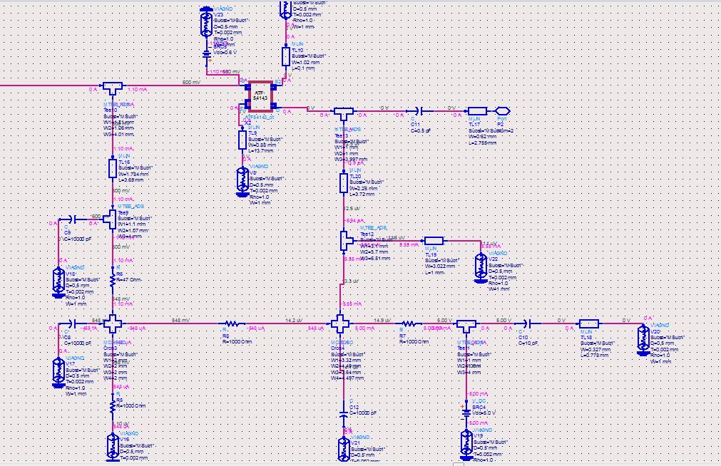
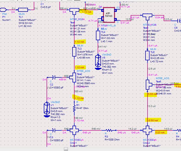
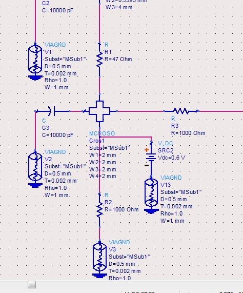
I used R1 and R2 for biasing. I used 0.6V bias source for simulation even so but there was no result again. What can be the reason, what mistake i did?


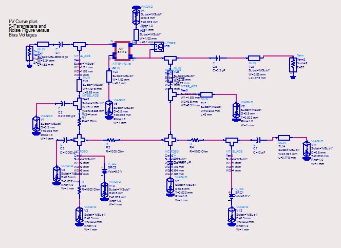
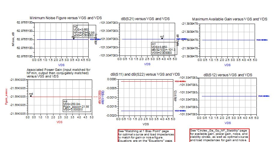
I simulated s-parameters on AWR so i need just OIP3,IIP3,P1dB and K.

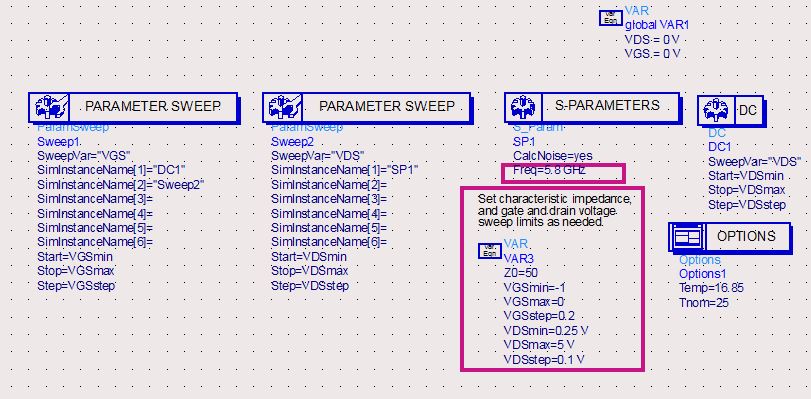
Also i added two tone harmonicsimulation but i haven't connect anything to it. Will i connect .s2p file and how?

Thank you.
 
Last edited:

That is only for the first stage device. You have not shown any DC sources connected to the second stage. Have you actually completed any DC simulation yet?

S-parameter device models will not be of any use for two tone HB simulations.
 

I used Avago application notes. I used passive bias so there isn't a source. Also the image wasn't the whole part, just bias souce added part.This is the whole schematic:
 

Which application note(s)? You have bais source connected to the first device, X1, but not the second device, X2. No bias sources are required for s-parameter simulation with s-parameter file models for the device which are measured at the required bias voltages/currents for the application but not the ATF54143_dt device model. This model is a non-linear GaAsFET device model and must have all appropriate bias source connected for it to work just as you have for X1. You really do need to complete DC simulations with these devices before to attempt any HB simulations.
 
Dear RealAEL,

1-Is it a problem if i don't use the same input and output matching networks for second stage? Because i designed this LNA on AWR and there were no problems and LNA has good s-parameter values.

2-what is wrong i couldn't understand. Can you have a look these images:


There is an absurd result for 2.scchematic. It is the same as i used for AWR.And It has 1.44 NF.
 
Last edited:

Those 2 images don't fit together. The circuit schematic is not set up to perform swept DC simulation that you have set up in the simulation controllers.

Also the I_Probe is short-circuiting the FET, connected between the drain and source. It would be better in series with the drain. Actually the I_Probe is not needed at all to do a simple (not swept) DC simulation and annotate the results to the schematic.
 

No I use two 5V supply voltage. But i want to ask this: for first stage i designed an input and output matching circuit but when i use the same matching circuits for second stage i can't get good results so i use a different,more simply, circuit. Do i have to use the same matching for second stage?


I am so confused. I used AWR and i got good results but in fact my designed LNA is rubbish when i try to simulate in ADS. And also i have limited time to do this.

Why my LNA doesn't work properly? what is wrong with the attached LNA? :-(
 
Last edited:

Why my LNA doesn't work properly? what is wrong with the attached LNA?

There are many things wrong. One mistake is the voltage supply of the second stange. If you have a cap between voltage source and transistor, how can supply current flow?

Also, see post #66 => current probe
 
There are many things wrong. One mistake is the voltage supply of the second stange. If you have a cap between voltage source and transistor, how can supply current flow?

Also, see post #66 => current probe

so many thanks volker@muehlhaus. I will change cap place.
 

I will change cap place.

Don't forget to change or remove the I_Probe.

You will also need to route bias to the gate pin of the device X2 also. As I posted previously once you have all the necessary connections you really need to complete a single point DC simulation at the normal bias voltage settings and then Annotate DC Solution back to the schematic to check that all the appropriate/expected voltage and current results.
 
OK.First off all i have to design a schematic correctly i think. I designed LNA schematic but when i smulate ATF-54143 has 0 A or -3.9aA. What can be the reason ?
 

What can be the reason ?

You have simulated the voltages and currents on the schematic? Why don't you look at these values, to see where the current goes? You will find the short circuits yourself by looking at the currents.
 

Agree with Volker. All the current is disappearing due to short circuits so no voltage is getting to the transistor therefore amplifier will not work.
 
Thanks.

OK I got it what you mean but i could not find why current drops to 0. If the reason is capacitor( because all current drops after caps) how can i solve this. I got help from agilent application notes.There shouldn't be any wrong.
 

Not the capacitors. Don't look at the current dropping to (near) zero. Look where the current is staying high. That is going instead of going to the transistors. That is the short circuit that should not be there.
 
Current is staying high through the microstriplines. do you think my layout can be wrong?


Don't just look at the gate bias, look at the drain. Start at the 5V voltage supply and see where the current goes. You have shorted your supply voltage to ground.
 
Status
Not open for further replies.

Part and Inventory Search

Welcome to EDABoard.com

Sponsor

Back
Top