Continue to Site

Welcome to EDAboard.com

Welcome to our site! EDAboard.com is an international Electronics Discussion Forum focused on EDA software, circuits, schematics, books, theory, papers, asic, pld, 8051, DSP, Network, RF, Analog Design, PCB, Service Manuals... and a whole lot more! To participate you need to register. Registration is free. Click here to register now.

Help need for drawing IIP3 and P1dB using AWR MICROWAVE OFFICE.

Status
Not open for further replies.
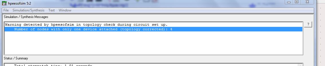
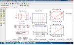
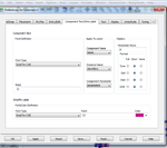
To get equivalent simulation results for two amplifiers connected in series the second amplifier should be operating at the same levels as the single amplifier case so that it is not being operated above compression. The Output power should remain the same. Therefore for two amplifiers in series the input power range should be reduced by at least the gain of the input amplifier, i.e.18dB or more. Reducing the Start and Stop power levels for both sweeps by 20dB should work.
 
RealAEL Sir
I am attaching the first stage LNA IIP3 results, two stage running result simulation execution result and diagram of sweep plan setting of two stage LNA. What exactly I need to do. I am sorry, what you said in the previous post, I didn't get sir. What I have to set for course sweep plan start = ? stop = ? step = ? and What I have to set for fine sweep plan start = ? stop = ? step = ? for two stage LNA to stop infinite execution simulation and to get IIP3 results as early.
 

Attachments

  • Simulation_Running_Result_Two_Stage_.png
    Simulation_Running_Result_Two_Stage_.png
    253.5 KB · Views: 99
  • Two_Stage_LNA_HB2_Two_toneswtpower.png
    Two_Stage_LNA_HB2_Two_toneswtpower.png
    320.1 KB · Views: 120
  • First_Stage_IIP3_MEASUREMENT_RESULTS.png
    First_Stage_IIP3_MEASUREMENT_RESULTS.png
    340.4 KB · Views: 107

RealAEL said:
Reducing the Start and Stop power levels for both sweeps by 20dB should work.

As I said just lower all Start and Stop sweep values in both course and fine plans by 20dB, i.e. current value - 20dB. Both the Step values would stay the same.
 

RealAEL Sir,
As you said I changed the start and sweep plan. Now it is working nicely without infinite loop and it will not take much time to execute. Thank you and thank you very much for your priceless help.
 

RealAEL Sir,
In third order IMD for IIP3 measurement, input power vs output power, I need to convert the rectangular plot to tabular data(Numerical values). How to convert the rectangular plot to tabular data plot ( Numerical values) for IIP3 measurement. Because I need the numerical values of input power, output power, first order and third order points to plot the third order intercept point externally using some software. Can you help me. Below show image red ring shows the rectangular plot.
 

Attachments

  • Rectangular to tabular plot.png
    Rectangular to tabular plot.png
    325.6 KB · Views: 108

If you have the data you want to see already plotted on a rectangular grid just swap that format with tabular format and you should be done. Simply right-click somewhere inside the area of the rectangular plot (not on the trace itself though) and then in the pop-up menu select Item Options at the top. For the Plot Type the first icon for the rectangular grid should be selected (on left). Change this to select the Tabular format icon (on right). Select OK to dismiss the UI and it should be done.

FYI - Once you have the Tabular style plot you can right-click on that and the bottom option is to export the data directly to an ASCII file, comma or tab delimited.
 
RealAEL Sir,
I have used the template of HB2ToneSweptPwr for my amplifier design measuring IIP3 and OIP3,and am getting following errors. How to resolve this errors for IIP3and OIP3 calculation.Showing error, I have attached below.
 

Attachments

  • IIP3_Measurement_Error_1.jpg
    IIP3_Measurement_Error_1.jpg
    334.5 KB · Views: 90
  • IIP3_Measurement_Error_2.jpg
    IIP3_Measurement_Error_2.jpg
    369 KB · Views: 89
RealAEL Sir,
Thank you for your help, whatever you have shown that link I have gone through. There they have given preventing convergence problems, they said you might have set out range of values, some other reasons also they have given. But they have given in ADS 2011, but I am using ADS2009. I didn't understand, what I have to avoid during design for not getting convergence problem. How to avoid the convergence problem,can you clear it.
 

Attachments

  • Convergence_Error.jpg
    Convergence_Error.jpg
    530.2 KB · Views: 90

Actually the link was to ADS 2012 but exactly the same information is provided for ADS 2009 (at the bottom of this page):

Analog/RF Simulation Computations and Convergence Criteria

I is impossible for anyone to give you any further instruction without doing a precise detailed analysis of your design and simulation setup. Just seeing the error message is of no use. What you need to do is what is listed in the document I linked to and the picture you attached:

•Turn on warnings.(default is no ). In ADS, set warnings on the Option component's Output tab.
•Act upon the messages in the Status window.
 
•Turn on warnings.(default is no ). In ADS, set warnings on the Option component's Output tab.
RealAEL Sir,
I am searching for the "option component Output tab". But I have searched in the Options > Preferences, couldn't find any component output tab.Where it is option component tab, where I have to go for getting this "option component output tab". There I have to go and turn on warnings.
 

Attachments

  • Options_Component_Output_tab.png
    Options_Component_Output_tab.png
    81.6 KB · Views: 88

From the component palette in the schematic window place an Options component symbol and then edit it and look at the Output tab.
 
Dear RealAEL,

I want to measure IIP3 of my designed LNAs which attached named LNA.rar. I understand that i must use ADS and I got 30 day trial license. I couldn't use atf54143_dt.dsn on ADS.I read what you wrote.Before doing these where should ATF54143_dt.dsn file be? Where should i copy this file? Because i could'nt find this file when i do what you said.


I really confused.Please help.


This is by far the easiest question you have asked so far. This is one of the basic operating modes of ADS. The custom symbol, when it is defined, is used whenever you the design itself is used in any design heirarchy. There are three easy ways to re-use any design but unfortunately one of them is not the palette.

Either of the following methods will work:

1. Open both the ADS main window and the schematic window where you wish to re-use design together. In the main window find the ATF54143_dt design in the "Project View" list. Now simply click and drag the design into the schematic window (keeping the mouse button held down). Click on the required location in the schematic window to place the symbol.
2. In the schematic window open the Component Library List. It is a button on the second toolbar that looks like a set of books or the menu command Insert > Component > Component Library... In the resulting window select the Projects line in the left panel. Again find the ATF54143_dt component in the right panel and click and drag it to the schematic window.
3. In the schematic window in the Component History toolbar dropdown list, the second one on the second toolbar next to the Palette selector list, simply type in the name ATF54143_dt and press enter. Again click the location in the schematic window where you wish to place the symbol.

Wire up the rmainder of the design and all is done.
 

Attachments

  • LNA.rar
    1.5 MB · Views: 86
Last edited:

For ADS 2009U1 and earlier it can be anywhere that ADS is configured to load component files, like biilt-in libraries or Design Kits, but the easiest place is in the networks sub-directory of the project that it open.
 

component library.JPG

i could nothing from now on. after i right click on atf54143_010407 on right panel "place component" appears and after click it an error occurs.
 

What error? Can't give you much help without more information.

Which version of ADS are you running? The fact that your previous screenshot shows "Workspace Libraries" and "ADS Analog/RF Libraries" etc. indicates that it may be ADS 2011.01 or later. ADS 2011.01 or later will not work with dsn files. These need to be migrated. Best thing to do in that case is contact Avago.

Your previous LNA.rar attachment also contains only .emp files and these are nothing to do with ADS.
 
RealAEL sir,

I measured s-parameters on AWR but it isn't enough. I learned that i have to measure OIP3,IIP3 and P1dB too. For these measurements now i use ADS2009. An error occurs when simulate. I am attaching what i have done untill now. Also do i have to connect 2tone harmonic to schematic ports?


Thank you so much. (sorry for my English:))


The error message tells you what is wrong. You are missing MSub1 so that means you have not placed an MSUB symbol in the schematic for use with the microstrip components. Fix that with a correctly configured MSUB and this error will not occur.
 
Thank you so much RealAEL.
i fixed some errors but i couldn't understand this error message:


Those are warnings not errors. Simulation will still run but somewhere in th design you have 4 unconnected pins. In ADS 2011.01 and later versions use Tools > Check Design... will give coordinates for these open connections (in ADS 2009 Tools > Check Representation... & test for Open connections)

Also the amplifier as you posted above will not work anyway for S-parameter or Harminic Balance simulations as you have not connected any bias sources. The models inside the devices are full non-linear models and not just s-parameter models.
 
Status
Not open for further replies.

Part and Inventory Search

Welcome to EDABoard.com

Sponsor

Back
Top