Continue to Site

Welcome to EDAboard.com

Welcome to our site! EDAboard.com is an international Electronics Discussion Forum focused on EDA software, circuits, schematics, books, theory, papers, asic, pld, 8051, DSP, Network, RF, Analog Design, PCB, Service Manuals... and a whole lot more! To participate you need to register. Registration is free. Click here to register now.

Help me to analyze this control circuit

Status
Not open for further replies.

mobinmk

Full Member level 2
Full Member level 2
Joined
May 27, 2010
Messages
140
Helped
4
Reputation
8
Reaction score
4
Trophy points
1,298
Location
Kollam (Quilon),kerala, India
Visit site
Activity points
2,484
Hi frndz,

am new bie here.

i wana to make variable frequency drive for 3 phase induction motor.
succesfully, i generate 3 pwm pulses using DDS by arduino uno.
nw i wana to make INVERT of 3 pulses.

spwm frequency is 33khz

first itz is fed into 12.5khz lowpass chebysck filter.
the output is fed into lm339 comparator.
vcc is 5v

output of the comparator gives two pulse which will AND ED WITH ORGINAL SPWM PULSES. USING 2 nand gate ic

i cant understant frm the lm339 comparator.

dc reference voltage by resistors fed into 3.3v??
output of comparator is connected with 2 resistor.in middle point =3.3v

why this 2 resistor is connected across the output of comparator.???
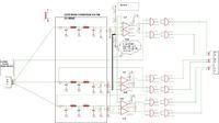
abc.jpg

pls reply.

regardz
mobin
 

i cant understant frm the lm339 comparator.

dc reference voltage by resistors fed into 3.3v??
output of comparator is connected with 2 resistor.in middle point =3.3v

why this 2 resistor is connected across the output of comparator.?

LM339 doesn't have an internal pullUp, so it needs an external one (s. LM339 dataSheet).
 
LM339 doesn't have an internal pullUp, so it needs an external one (s. LM339 dataSheet).

Thnkz bro.

can i use external supply means to nand gate ic ??
vcc of lm339 is 5v.

vcc of NAND GATE IC is 10v and GND is isolated.
-------------------------
what happen if i connect the output of comparator with nand gate ic without pull up resistor.can u explain in detail
-------------------------
Thnkz bro,
can u explain this circuit after the lowpass filter in detail?
 
Last edited by a moderator:

The circuit is incomplete. CD4011 power supply is missing.

CD4011 GND must not be isolated from comparator ground. CD4011 input high level must be 70 percent of it's supply voltage, this can be achieved by connecting the pull-up resistors to the CD4011 supply. The circuit doesn't work without pull-up resistors.

Thnkz for your valuable reply.

I have another doubt.

output of cd4011 is fed into driver ic (IR2110 or IR2336).

Can u recommend the VCC supply voltage to cd4011 ic ?? 5v?? 15v??

Can i isolate the cd 4011 ic frm ir2110 driver ic ??

Spwm Frequency is 33khz.

which optcoupler is used ??

regardz

mobin
 

Requirement for isolation is often imposed by the application, e.g. high voltage DC bus or strong interferences. It's hard to determine without knowing the design details. There are many fast optocouplers available on the market for this purpose. You usually also need a second isolated power supply.

Logic level to drive IR2110 can be anything between 5 and 15 V (theorectically even down to 3.3V, but timing performance is rather bad below 5 V), the driver IC should use the same supply as IR2110 Vdd.
 
Thnkzz bro.
dc link voltage is 500v.
Any difference in timing perfomance of IR2110

1) Vdd is 5 v & Vcc is at 15v.

2) both Vdd & Vcc is 15v .

SPWM frequency from cntroller is 33khz .

Can you recommend which optocoupler is better ??
pc 817??
 

The circuit is incomplete. CD4011 power supply is missing.

CD4011 GND must not be isolated from comparator ground. CD4011 input high level must be 70 percent of it's supply voltage, this can be achieved by connecting the pull-up resistors to the CD4011 supply. The circuit doesn't work without pull-up resistors.

Thnkz Bro.

i have doubts.

the input is 3 spwm signals frm aurdino uno.

itz frequency is 33khz,

first it fed into 12,5khz low pass cheybsck filter

**broken link removed**

the ouput of three low pass cheybsek filter is

3 sine wave with 120 deg each other.

so nw i wana to make 6 pulses ( 3 pulses - a,b.c & invert of 3 pulses a^,b^,c)

pls explain in detail frm the input of lm339 a comparator.
 

[Moved]Help Me To Find mistakes in this Circuit (LM339 SECTION)

Hi Frndz.

Am new bie here, I wana to make VFD of 3 phase induction motor , The 3 SPWM pulses generated by ARDUINO UNO

by reference dds generator

**broken link removed**

ok nw i wana to generate invert of 3 pulses.

spwm frequency is 33khz,

abc.jpg

first filter the 3 pulses using 3 low pass cheybsck filter at 12.5khz.

output of filter is 3 sine wave which is 120deg phase shift with each other.

upto lowpass filter i belive that the ckt is correct.

if any mistakes in the lowpass cheybsck filter section pls notify me.

1) why 100k potentiometer is connected in the output of low pass chebysef filter ??


can i vary the amplitude of sine wave ??

Next section is lm339 comparator ,

output of 1st low pass filter is connected to the +ve terminal of IC1B (comparator) & -ve terminal of IC1A( comparator).

similarly 2nd , 3rd low pass filter is connected to the coressponding terminals of IC1C,IC1D and IC2A,IC2B.


the other terminals of IC1A is +ve and -ve of IC1B is connected to potential divider making 3 resistor to +3.3v.

2) can i supply 5v to the vcc of LM339 ic ??

3) Is design value of 3 resistor to make potential divider across +3.3v and grnd be same ??

resistance value depend dead time ,duty cycle ??

Now the +ve terminal of IC1C & IC2A is connected to the IC1A.

BUT the -ve terminal of IC1D,IC2B is jus short each other, Any mistake there ??


I think that -ve terminal of IC1D,IC2B is connected to IC1B ??

output of lm339 comparator is pull up to +3.3v

next in CD4011 SECTION VCC ,GRND is missing.

4)how much voltage supply to the vcc of cd4011 ??

5) why the orginal pulse 33khz is NAND ed with Output of comparator ??


Regardz

mobin
 
Last edited by a moderator:

The DDS link finally clarifies how you arrived at the circuit in post #1.

Unfortunately it's the wrong attempt to make a motor inverter. In stead of low pass filtering the pwm output, it would be directly send to the power stage. Appropriate logic must provide dead time for the gate signals, avoiding simultaneous on-state of high and low side transistors.

A side node about opto coupler. PC817 is a slow optocoupler with many µs rise and fall time and respective delay and delay skew. You need a fast optocoupler with logic gate output and MHz speed.

THnkz bro.

pls recommend the optcoupler ic ??

pls see this report which i attached.

can i use NOT GATE IC to get inv of 3 pulses .


regardz

mobin
 

Attachments

  • Design Strategy for a 3-Phase Variable Frequency Drive (VFD).pdf
    807.4 KB · Views: 80

I was assuming so far that you want to drive the motor with sine alike voltage. The circuit in post #1 can work to generate a square wave. But driving the motor with a three-phase square wave (similar to a simple BLDC drive) can be achieved much easier and won't need all the sine generator stuff.
 
Thnkz bro,

Nw my project is about 50%, and got all components .

output of low pass filter is connected with potentiometer thus i can vary the duty cycle.

frequency can vary by varying potentiometer in aurdino uno.


So i wish to continue,

Can u reply the post #9 ??

Regardz

mobin
 

[Moved]Suggest me to choose optocoupler ic, SPWM frequency is 33khz

Hi frndz,

Am looking for your valuable replies.

I wana to design an optcoupler circuit b/w cntroller ckt frm driver ic IR2110.
SPWM frequency is 33khz.

Which is cheap and available..

plz share your knowledges

regardz
mobin
 

The duty cycle is primarly defined by the sine waveform. I guess you want to change the sine magnitude, but this should be done by a multiplication in the arduino software. Please consider that a proportional v/f characteristic should be implemented, don't apply full voltage at low frequency.

Regarding not-gate usage. The gate signals for low and high side driver are basically complementary. But you need assure a certain dead time between low and high side on-state. Some gate drivers have build-in deadtime, it can be also achieved by assymetrical gate circuits (resistor + diode) or by an asymmetrical delay with a RCD circuit in front of the driver IC.

- - - Updated - - -

Optocoupler: e.g. Sharp PC400, PC410, Toshiba TLP109, TLP118, many vendors 6N137

Thnkz Fvm..

for your valuable reply.


1) Can i use IR23364 driver ic ??

datasheet

**broken link removed**

Another doubt is

2) Why output of lm339 is NAND ed with Orginal pulses ??

In post #9
"
Now the +ve terminal of IC1C & IC2A is connected to the IC1A.

BUT the -ve terminal of IC1D,IC2B is jus short each other, Any mistake there ??


I think that -ve terminal of IC1D,IC2B is connected to IC1B ?? "


Now i modifed the circuit

plz check


any mistakes ??

Regardz

Mobin
 

I keep my opinion from post #10 that the low-pass and comparator combination is not useful to drive a motor inverter.

I must confess that I still don't understand what you want to achieve by ANDing the pwm input with the comparator output. Apparently the sine modulated pwm is processed in two parallel pathes, but why?
 
Thnkz Fvm

i think that

The square wave is then fed into an input to an AND logic gate. Available on hand were NAND gates, a buffering NAND gate was added in an inverting configuration to replicate the behavior of an AND gate. The other input is the original unfiltered PWM output from the Arduino board. This allows the square wave to act as an enable for the signal to pass only when desired. When both the PWM and the enable are high, the logic output will be high. When one is low, the output is low. The resulting signal is a replica of the enable signal, but instead of being consistently high for a given duty cycle, the PWM will be visible during this time. There will be three of these filtering circuits and six control signals will be produced. Two signals from a single filter correspond to a single phase. These signals are then fed into a gate driver.

pls check the modifed circuit in post #16
"
Now the +ve terminal of IC1C & IC2A is connected to the IC1A.

BUT the -ve terminal of IC1D,IC2B is jus short each other, Any mistake there ??


I think that -ve terminal of IC1D,IC2B is connected to IC1B ?? "


today,i checked the output of low pass filter in DSO

peak to peak voltage is 2.45v without 100k pot

nw i want to make 2 pulses( a,a^) using lm339 ,

the output of low pass filter fed into - terminal of IC1A(1st comparator) and +ve terminal of IC1B(2nd comparator).

nw i try to design the value of voltage divider , which 3 resistor R1,R2.R3. across +3.3v and grnd.

Let the voltage V1 at the middle point of R1 and R2 connected to the +ve terminal of IC1A(1st comparator).

and the voltage V2 be between the resistor R2 ,R3 be connected to - ve terminal of IC1B(2nd comparator).

see the ckt.

Design of resistor value is depend on dead time.

in order to make exact complement of pulses (a,a^)

R1 = R3, R2= 0.
nw V1=V2.

Is it correct ???

am waiting for you reply.

regardz

mobin

- - - Updated - - -

Dear FvM

My project is completed upto low pass filter section.

nw i wana to move to lm399 section. to generate two logic pulse (a ,a^)

Nw,i faced 2 prblms

1) is this modifed circuit is correct ?

In orginal circuit ,i noticed that -ve terminal of 4th & 6th comparator is shorted each other not connected to the voltage divider or -ve terminal of 2 nd comparator.

2) Design of voltage divider ( value of R1,R2,R3) ,considering dead time. how much dead time will consider ?? 3us??


Regardz

mobin
 

Attachments

  • abc.jpg
    abc.jpg
    161.1 KB · Views: 90

Status
Not open for further replies.

Similar threads

Part and Inventory Search

Welcome to EDABoard.com

Sponsor

Back
Top