Continue to Site

Welcome to EDAboard.com

Welcome to our site! EDAboard.com is an international Electronics Discussion Forum focused on EDA software, circuits, schematics, books, theory, papers, asic, pld, 8051, DSP, Network, RF, Analog Design, PCB, Service Manuals... and a whole lot more! To participate you need to register. Registration is free. Click here to register now.

Help in sizing OTA(VCCS) for LDO

Status
Not open for further replies.

roki

Member level 1
Joined
Mar 29, 2009
Messages
33
Helped
0
Reputation
0
Reaction score
0
Trophy points
1,286
Activity points
1,545
Hi everyone,

untitled.PNG

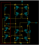
Attached is the OTA schematic i've drawn.
My first question is whether the type of current mirror(red boxed) i used to generate a cascode bias voltage is correct or incorrect?
Then next, i need help in designing all transistors to be in saturation.I tried myself numerous times, but kept failing.
Highly, the way i calculated it is very wrong.The supply voltage is 1.2V, thus it does make it harder to design due to small headroom.
Bias current is 1uA.Kindly assist me in designing all transistors to be saturation.

Thanks
 

... i need help in designing all transistors to be in saturation.I tried myself numerous times, but kept failing.
Highly, the way i calculated it is very wrong.The supply voltage is 1.2V, thus it does make it harder to design due to small headroom.

What are the threshold voltages Vthn, Vthp of your MOSFETs? With your architecture, you need a power supply
VDD > 3*Vthn+1*Vthp to work properly. I think such a "double-stack" architecture doesn't leave enough headroom with a 1.2V power supply, so isn't well appropriate.

BTW: the 2 bottom-most and the 2 top-most FETs of the amplifier desirably should be in saturation, too, but don't necessarily have to be so (less gain, then).
 

The threshold voltages for Vthn and Vthp is 0.3V.
And by plugging the the values into the VDD > 3*Vthn+1*Vthp, it does come up to 1.17V,so 1.2V of supply is enough.
My calculations based the pre-assumed Vds of each transistors to 0.2V-0.3V,in which to allocate headroom do not help at all.The transistor sizing(w/l) that i pre-calculated based on the Id and Vds assumption is not even close to the simulated results.
Does the "double stack" refers to cascoded?
 

The threshold voltages for Vthn and Vthp is 0.3V.
And by plugging the the values into the VDD > 3*Vthn+1*Vthp, it does come up to 1.17V,so 1.2V of supply is enough.

30mV Vds headroom for 4 transistors? I don't think so, it can't work!
Minimum headroom in order to work in saturation is 4*Vt ≈100mV (@RT, per transistor), and this just in deep weak inversion (subthreshold) mode.

Does the "double stack" refers to cascoded?
Yes. Double cascode, for input & output.
 

0.3V is 300mV.So shouldn't it be enough since the minimum is 100mV?

I'm attaching the dcop simulation results of each transistor for your reference.
The first figure is the upper mosfet and the second is the bottom mosfet.
Kindly look through
Thanks!
1_1.png
1_2.png
 

0.3V is 300mV.So shouldn't it be enough since the minimum is 100mV?
Even 300mV isn't enough to get 4 -- or even 5 -- stacked MOSFETs into saturation.
But ...

... VDD > 3*Vthn+1*Vthp, it does come up to 1.17V,so 1.2V of supply is enough.
... in my math, 1.2V - 1.17V = 0.03V = 30 mV
 

To bias Vb1, it is better to use PMOS instead of NMOS?
 

I suppose it is quite impossible to design this circuit with a supply of 1.2V. Is there an alternative to implement this VCCS with such a low supply?How about if i were to implement self-biased cascode?

@leo_o2:Hi, even if i were to use a PMOS instead of a NMOS, will there be a significant difference?
 

I suppose it is quite impossible to design this circuit with a supply of 1.2V.

I think so. Sameer Somvanshi & Santhosh Kasavajjala describe a similar topology, but just 4 stacked MOSFETs with a 1.8V supply (Vref≈465mV). Unfortunately there's no min. operating VDD given. Process was 0.18µm CMOS, Vth=435mV, however.
 

Checking only the typical conditions is not sufficient. Please think about a corner case with low Vdd and high Vt ("slow corner").
 

Checking only the typical conditions is not sufficient. Please think about a corner case with low Vdd and high Vt ("slow corner").

That's very true, Michael, but I think at design start you have to size the transistors for DC conditions which first of all center the design for TT conditions, isn't it?
If this works well you'll test the corners and possibly change and try to keep it centered within the corners' frame.
And then run the Monte Carlo sims ...

Yes for sizing, of course. But when thinking about whether a topology's stacked transistors' Vth will fit into Vdd, it's reasonable to take the upper worst-case of Vth and the lower worst-case of Vdd into consideration right from the beginning. If this test fails, you don't have to size anything but take a different topology.
 

... If this test fails, you don't have to size anything but take a different topology.

Yes, you're right, Michael. Midwhile I had forgotten the original "double stack" cascode topology with VDD=1.2V , sorry!
 

Status
Not open for further replies.

Part and Inventory Search

Welcome to EDABoard.com

Sponsor

Back
Top