bkat
Member level 2
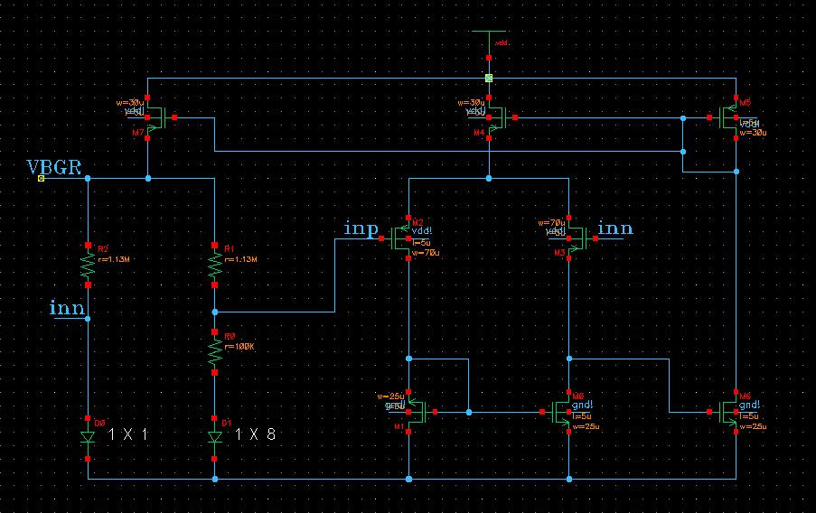
1 how to design this error amplifier?? (bandwith?? gain?? offset?? noise?? )
2 how to simulate the error amplifier independently??
3 how to simulate the PSRR of this BGR?
Thx
Regards
bkat
Follow along with the video below to see how to install our site as a web app on your home screen.
Note: This feature may not be available in some browsers.
bkat said:1 how to design this error amplifier?? (bandwith?? gain?? offset?? noise?? )
2 how to simulate the error amplifier independently??
3 how to simulate the PSRR of this BGR?
Thx
Regards
bkat
bkat said:
1 how to design this error amplifier?? (bandwith?? gain?? offset?? noise?? )
2 how to simulate the error amplifier independently??
3 how to simulate the PSRR of this BGR?
Thx
Regards
bkat
isaacnewton said:Where did you find this circuit? Could you provide the reference for this circuit? Thanks.
bkat said:
1 how to design this error amplifier?? (bandwith?? gain?? offset?? noise?? )
2 how to simulate the error amplifier independently??
3 how to simulate the PSRR of this BGR?
Thx
Regards
bkat
isaacnewton said:It looks like some PMOS and NMOS transistors are misused.
szekit said:1) the second stage of the amp is diode-connected load. it will decrease your gain. i guess the overall gain is around ~30dB?!
2) high bandwidth amp can give you better supply noise rejection in Mhz frequency range. high dc gain can give you a good bandgap voltage independent of PVT.
bkat said:thanks ycj mince
Can you told me why error amplifier should be high gain and low bandwidth.
And in my opinion this amplifier's gain is about 50db .
Can you give me some advice no how to improve this BGR?
Regard
THX
bkat said:but the diode-connected make the bias current of the opamp independent of PVT
thanks
bkat said:no need the start up circuit
bkat
ipsc said:bkat said:but the diode-connected make the bias current of the opamp independent of PVT
thanks
Independent of PVT?????
Diode connected current≈2*BJT current.
Though BGOUT has ~ZERO temp. coefficient, BJT current=ΔVd/R0 will have +ve temp. coefficient.
And the current will be process independent only if 'R0, R1, R2' are process independent; which won't be the case unless 'R's are external resistors. An onchip resistor will vary as much as 25% across process. So does the current.
point me if i am wrong.
Added after 4 minutes:
bkat said:no need the start up circuit
bkat
Did you ramp the VDD and check?
Regards
bkat said:off course the diode-connected will decrease the gain.but the diode-connected make the bias current of the opamp independent of PVT
thanks