Continue to Site

Welcome to EDAboard.com

Welcome to our site! EDAboard.com is an international Electronics Discussion Forum focused on EDA software, circuits, schematics, books, theory, papers, asic, pld, 8051, DSP, Network, RF, Analog Design, PCB, Service Manuals... and a whole lot more! To participate you need to register. Registration is free. Click here to register now.

Help! Can someone clarify to me how this converter circuit works?

Status
Not open for further replies.
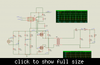
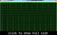
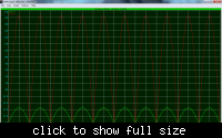
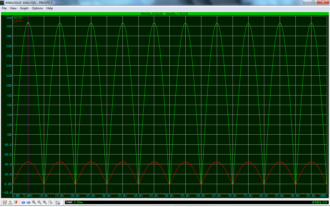
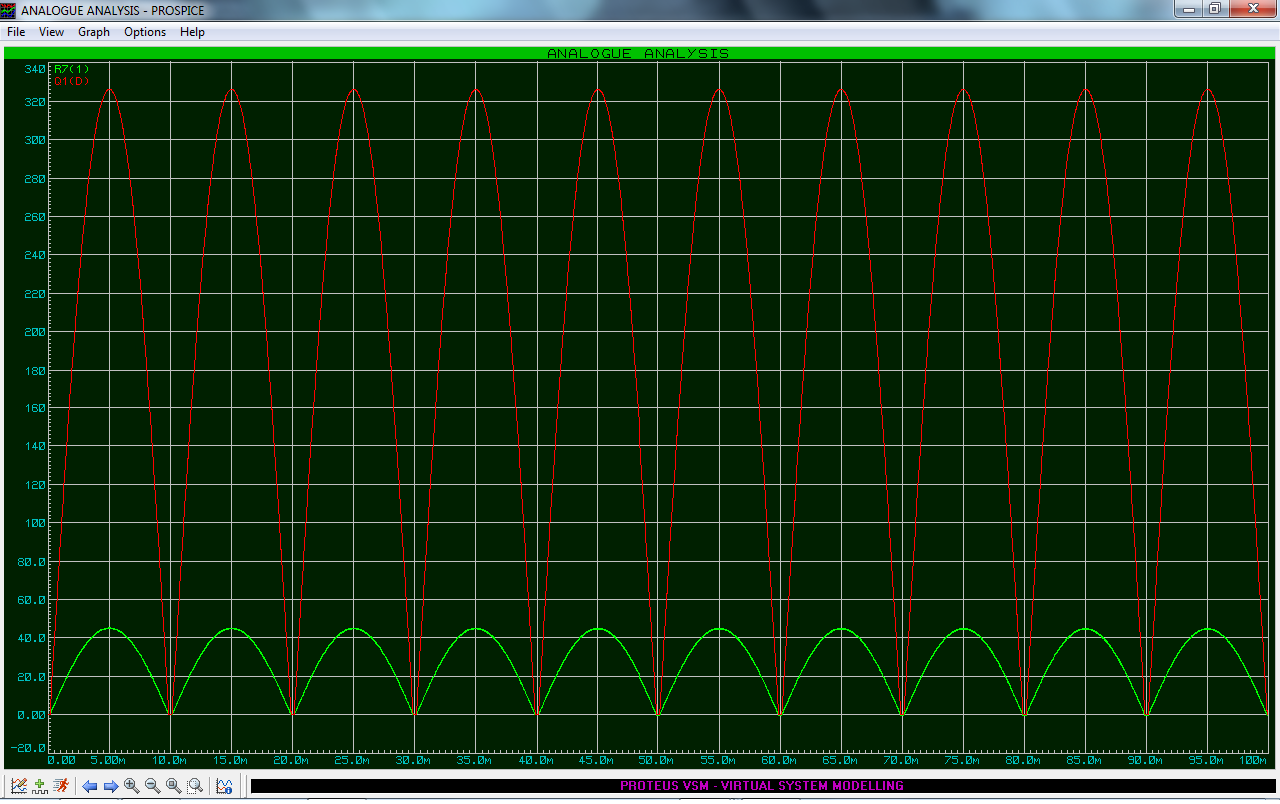
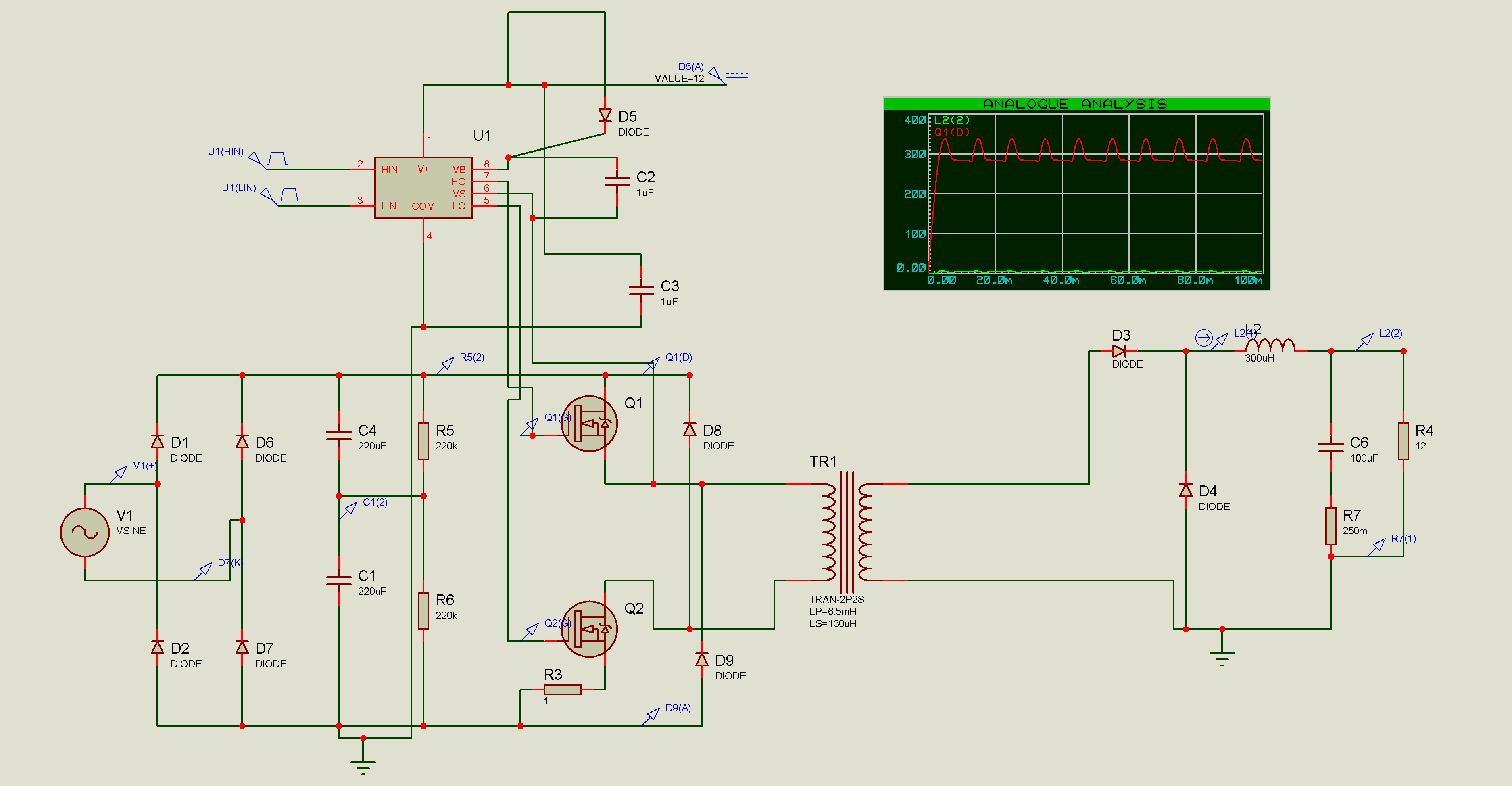
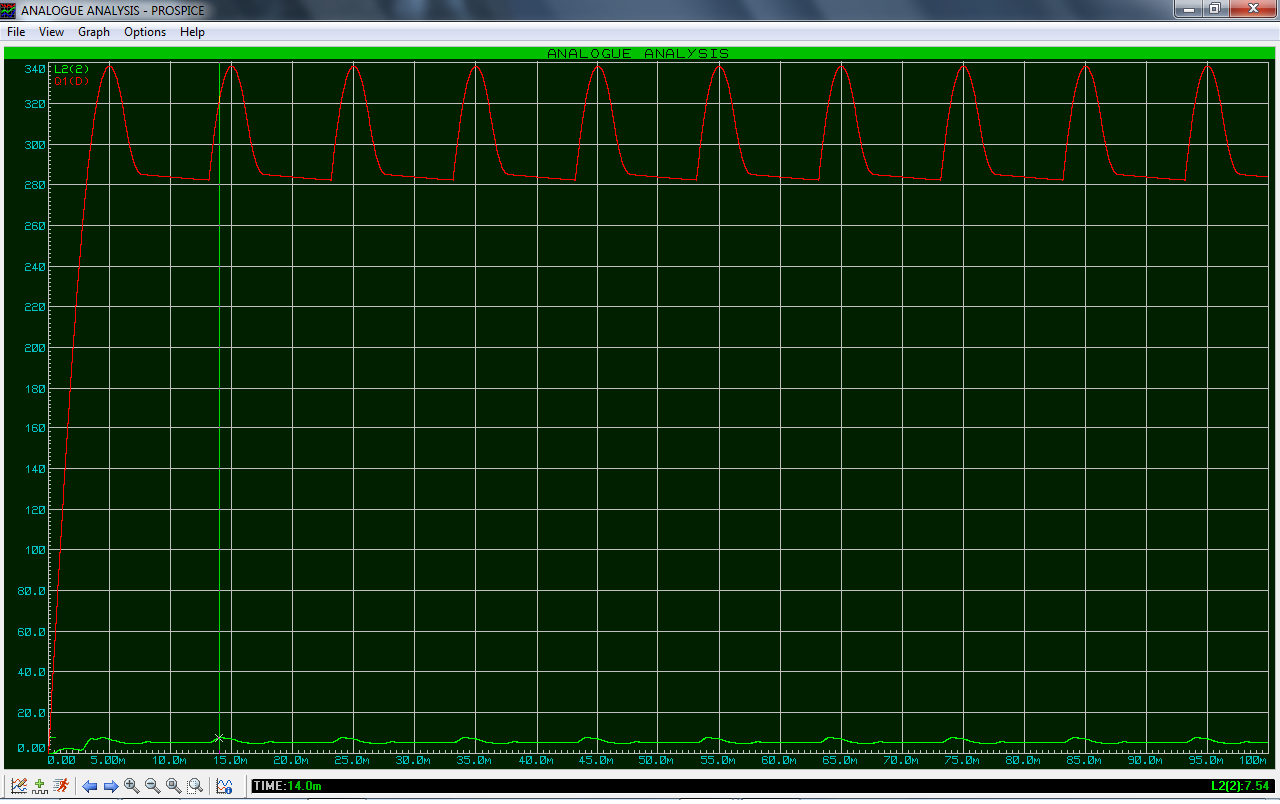
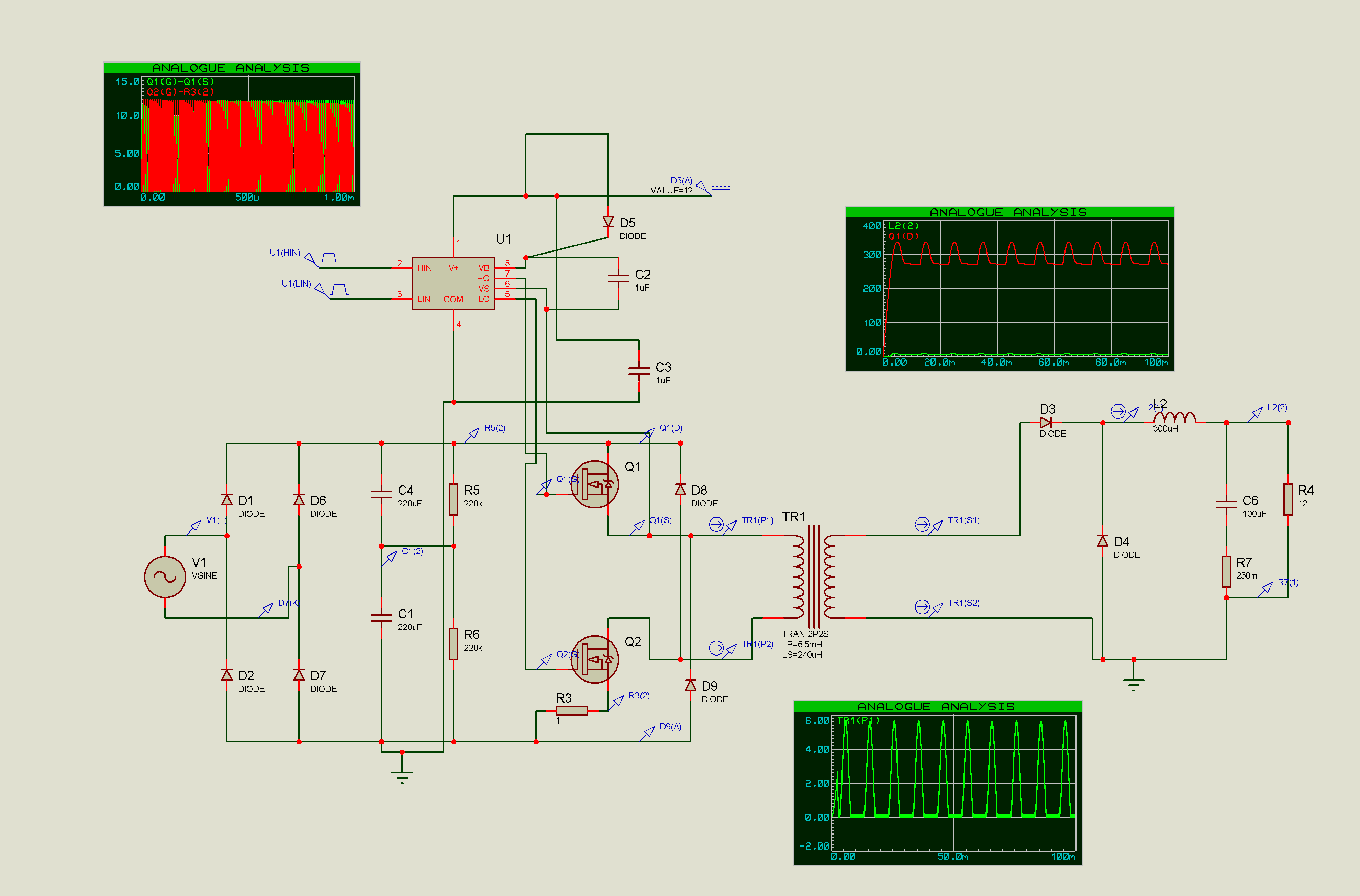
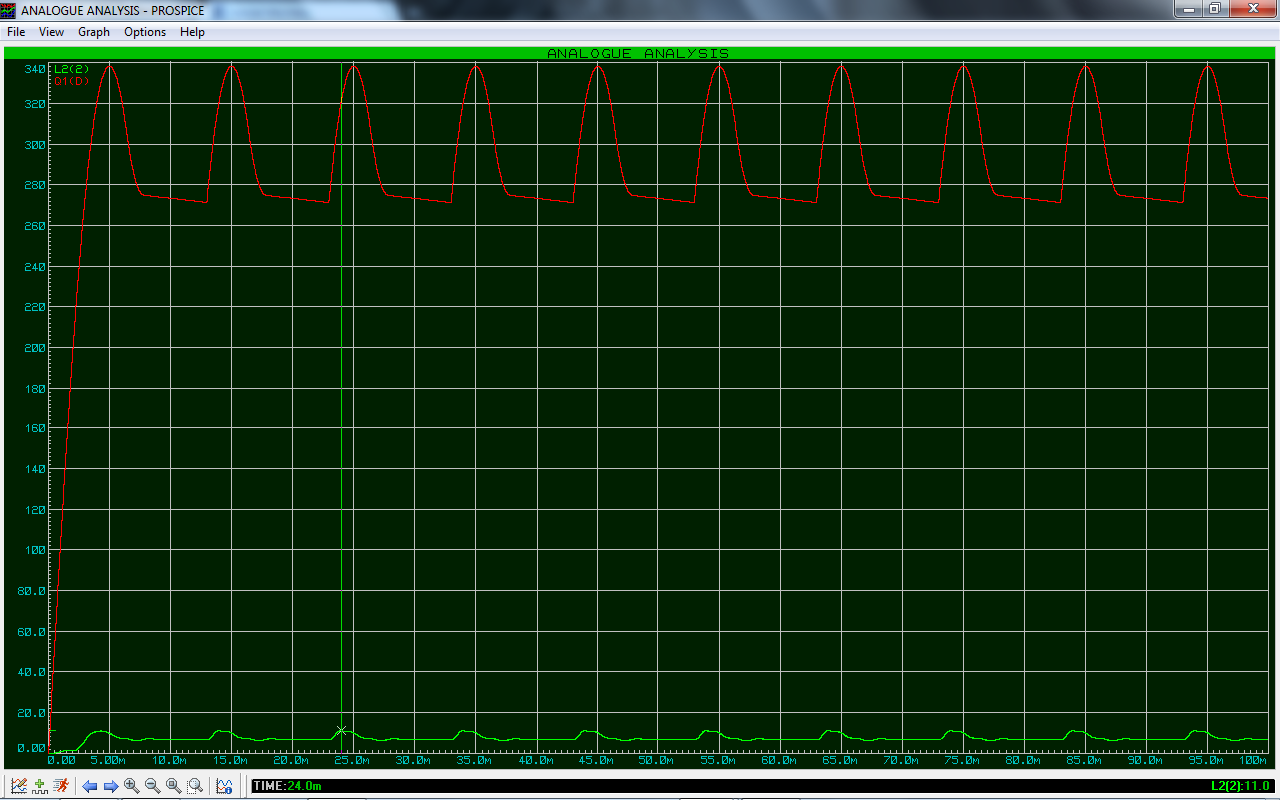
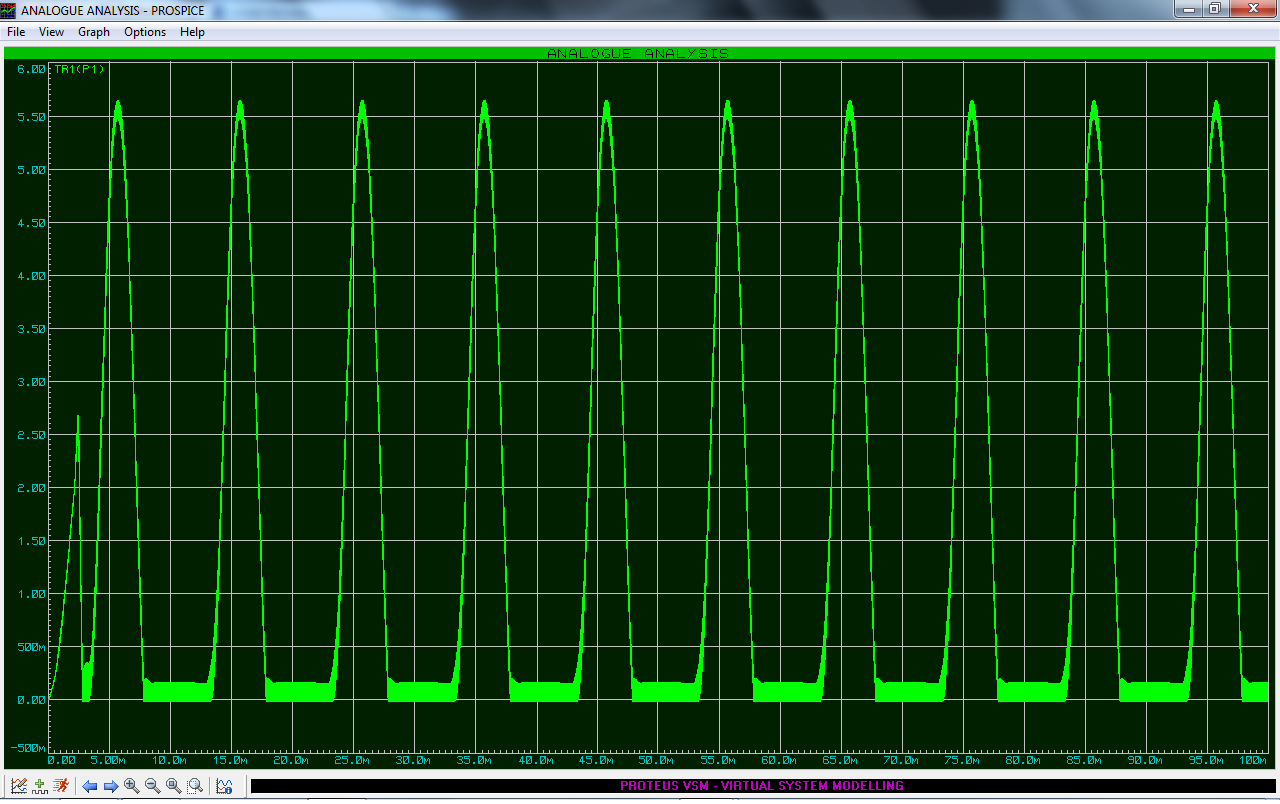
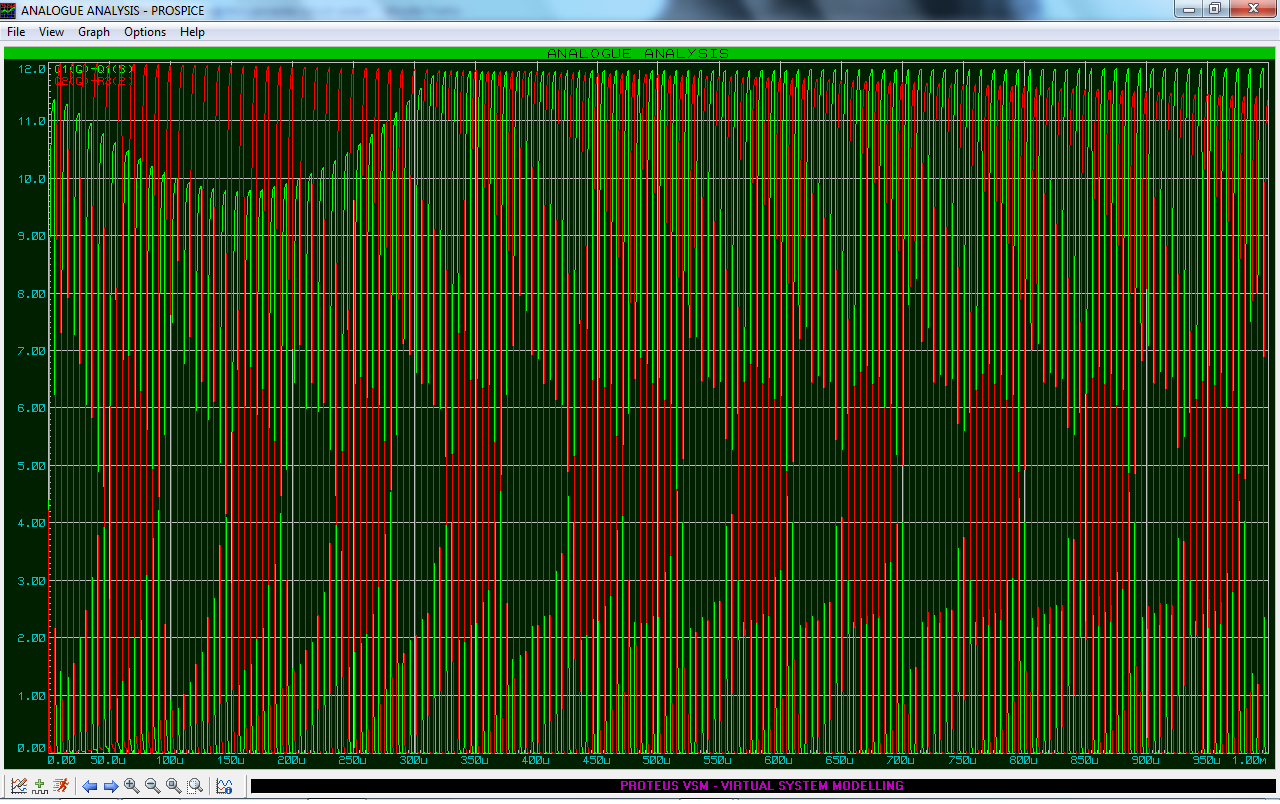
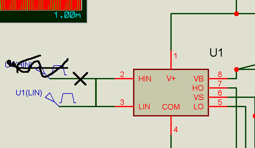
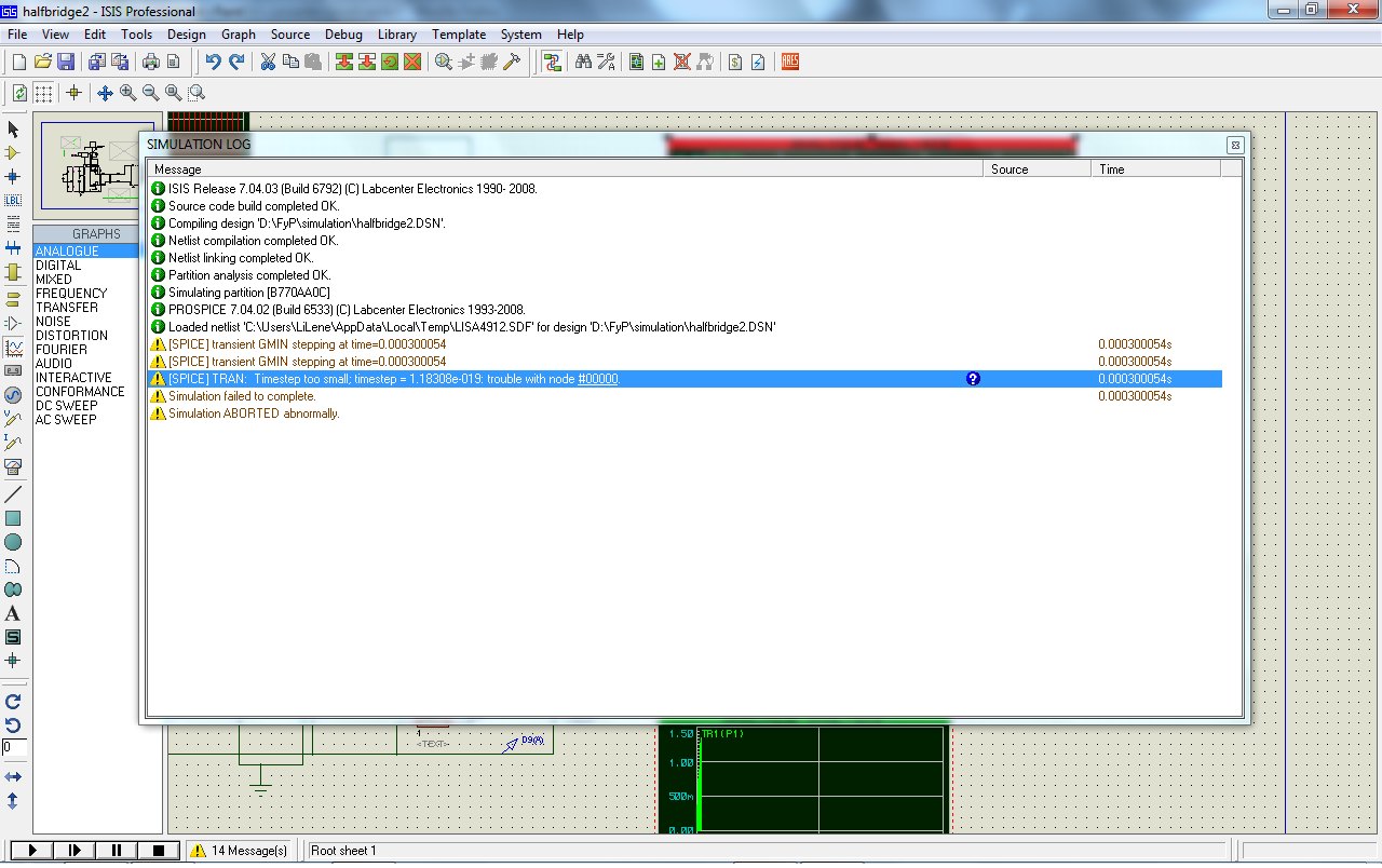
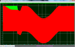
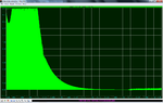
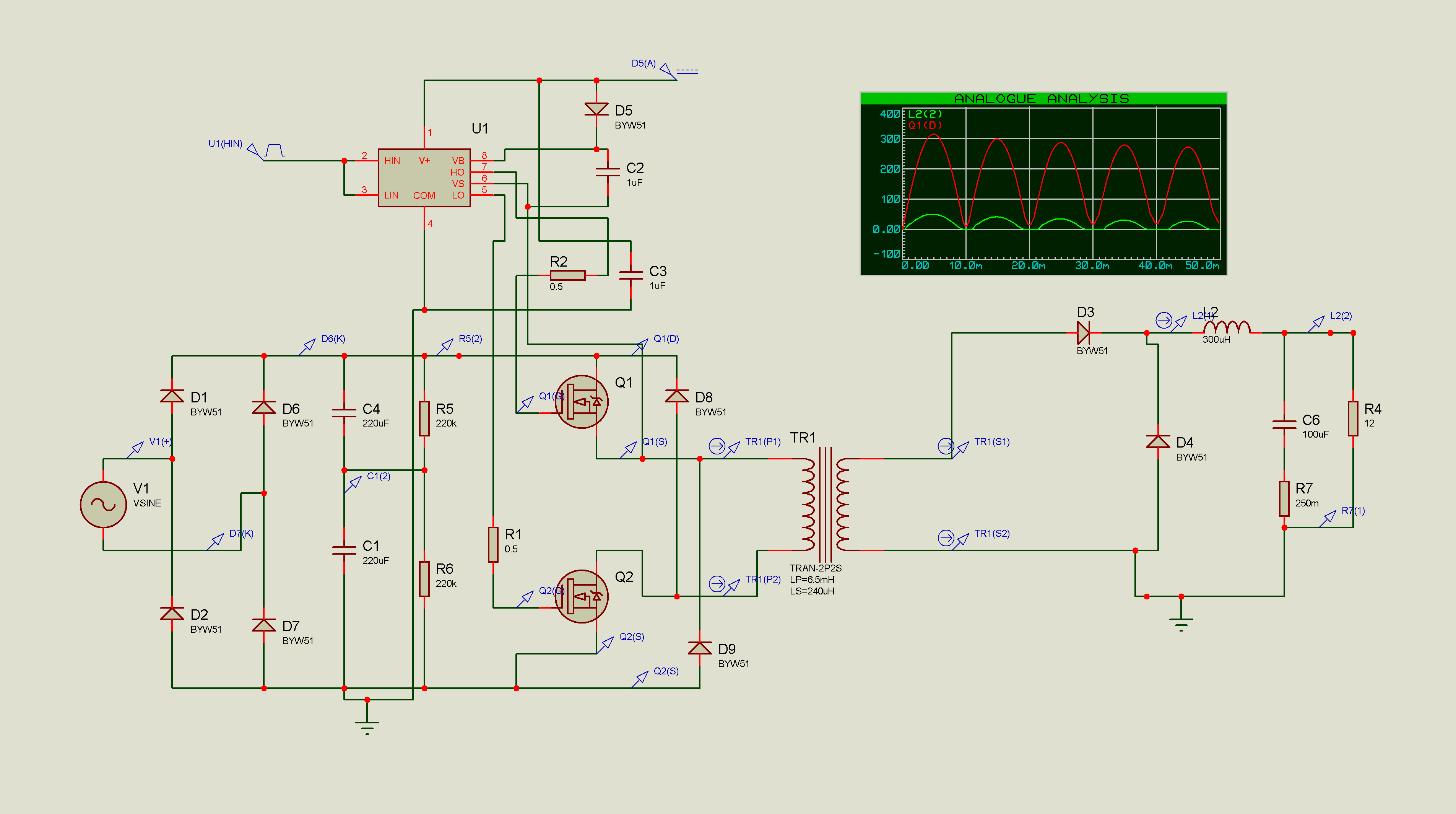
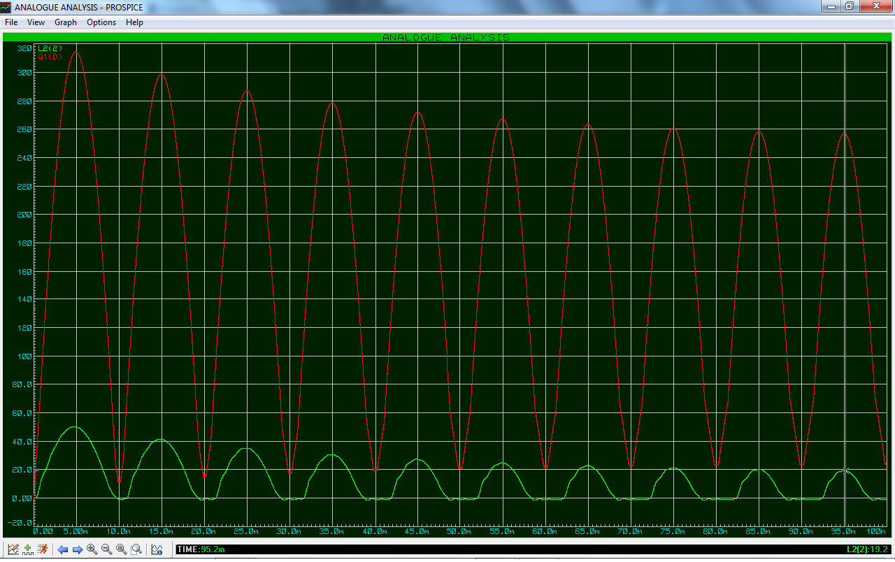
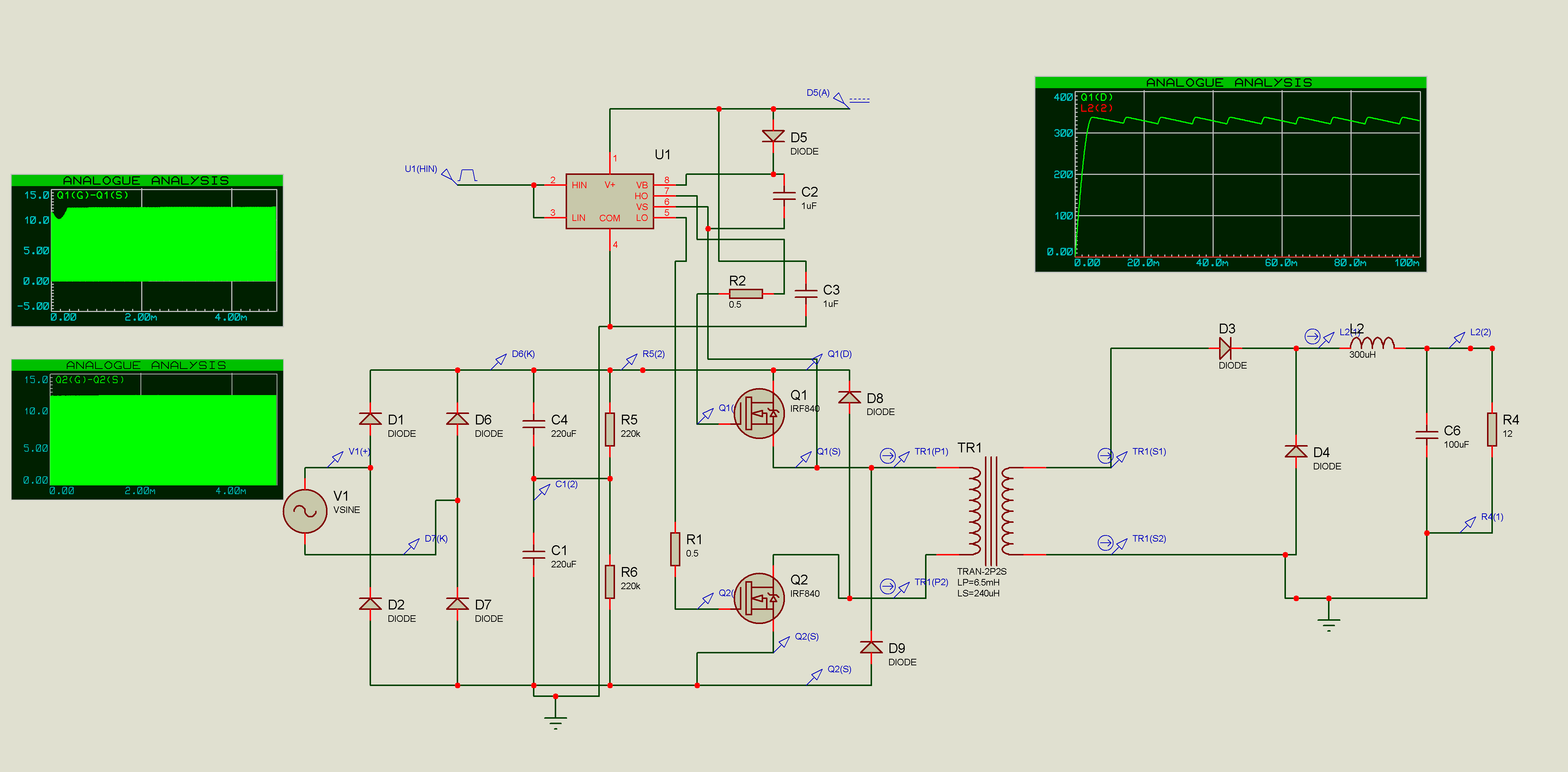
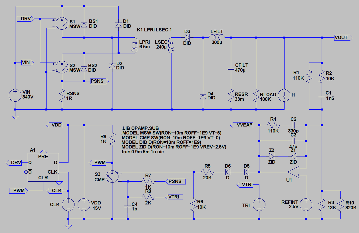
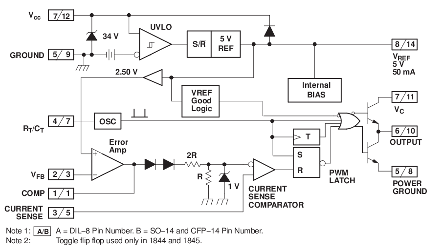
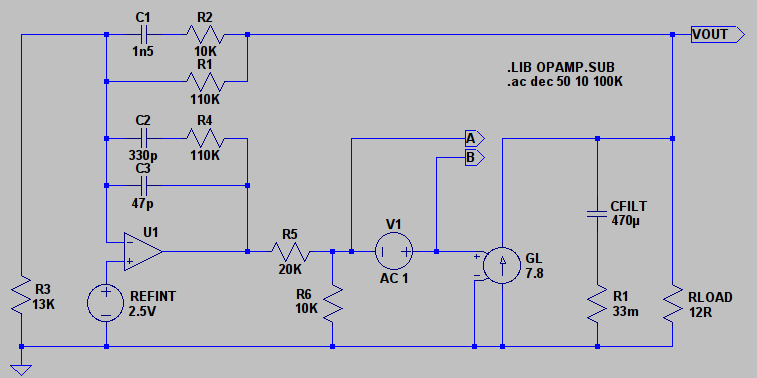
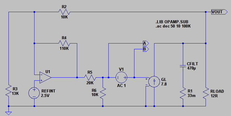
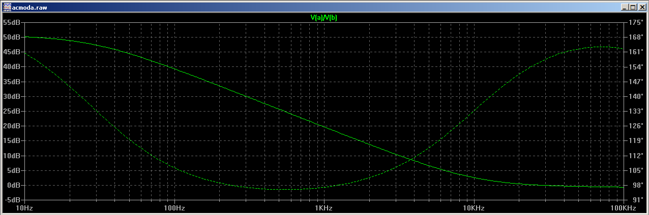
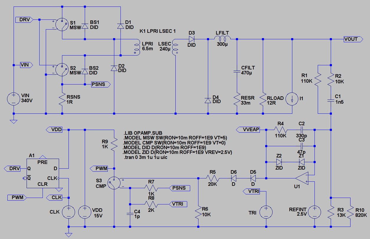
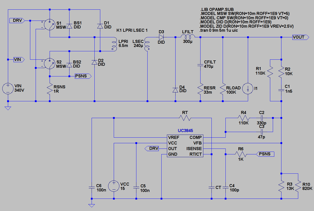
Hi, Genome. Unfortunately, the transformer that I'm using need to have that connection. Now, I have changed a new transformer. The primary Vp=340V and Vs=48V. So, Lp=6.5mH and Ls=130uH. Below are the circuit and waveforms I obtained. I can get roughly 45Vpeak but referring above, you mentioned that the output should be 24V due to the 50% duty cycle. But do this duty cycle affect the voltage since this is not a dc-dc chopper. Since the circuit has a LC filter, there should be smoothing voltage output but I just get full wave. Am I taking the wrong output?


Hello Again.

You have removed the connection as shown in my last picture but you were supposed to reconnect it to circuit ground. Try this,


From your waveforms, Q1C in particular, it looks like you have both Mosfets permanently switched on and are effectively shorting the input supply through the transformer primary. Can you check that the gate drives are correct. You should have something like a 12V 50% duty cycle pulse waveform at 100KHz.

Genome.
 
This is the corrected circuit. The output voltage is about 7V-8V but not 12V.


Looking better.. Make the rise and fall times of your U1(HIN) and U1(LIN) sources 50nS. If your transformer primary is 6.5mH then your secondary should be 240uH. Can you post a picture of the voltages Gate to Source of Q1 and Q2 just to verify that U1 is doing its job properly and also what the current in the transformer primary is doing. Also what is U1 'modelling'. I realise it is a level shifting gate driver but which particular device. There still seems to be quite a lot of ripple on that input supply but things seem to be waking up..

Apologies for asking lots of questions.

Genome.
 
Thanks, Genome. It's alright to ask questions so that I can improve and solve the problems.

Now my Vpeak is 11V after changing Ls=240uH. The driver is IR2101. Yea, it seems to have quite large ripple.


Nice one.

I think


Tells a tale and might be an indication of things 'misbehaving'.

You can see the Q1 Vgs 'making its mind up'. It's probably the case, and I might be wrong, that you have things set up so before the analysis runs the software solves the DC operating point. That gives the IR2101 the 'right' voltage via D5 to C2 for it to run. When things do get going, and they are not doing it properly yet, you get a 'drop' in the C2 voltage before it charges up again.

Otherwise it looks like you are still thinking in terms of driving a 'half bridge' circuit where Q1 and Q2 get switched alternatively. For this one they should be switched together. You might still have the driving sources set up to work with the half-bridge circuit.

Try,


Genome.
 
Hi, Genome. I would like to ask that this circuit is no longer a half bridge? It is just a AC to DC converter?

After I changed the Q1 and Q2 switch together, the circuit cannot be simulated. I keep getting load partial results.
So, I changed the GMIN The result is still the same as I posted earlier. I think it might due to the driver because the Vgs are not constant.


Attachments

  • Untitled2.png
    Untitled2.png
    179.1 KB · Views: 96
  • 3.png
    3.png
    102.9 KB · Views: 90
  • 4.png
    4.png
    92.1 KB · Views: 86
  • 5.png
    5.png
    91.5 KB · Views: 92
Last edited:
The circuit is no longer a 'half-bridge' it is now a 'Two Switch Forward Converter'. Both are Offline DC to DC converters. You are feeding them with AC but really since that is rectified and smoothed it is really DC.

Aha.... Nasty.

Going back to,


I've just realised that you have plotted the transformer primary current as I requested but I was not paying attention. Sorry about that one. Looking at your latest waveforms. Yes it does look like the driver is having problems particularly the upper gate drive is not getting properly charged. I'm not sure I can rationalise what the lower gate is doing going negative with respect to its source... scratches head. Ah! Going back to your transformer primary current. It is getting up to 5.5A, which is not good, and it is the 5.5A flowing through R3 that is resulting in the gate of Q1 going negative 5.5V with respect to the source. That is also what is producing the large ripple on the input filter capacitors, C4 and C1.

Things are making sense, they are just not working correctly. Go back to your U1 voltage source,


and, keeping the rise and fall times at 50nS make the pulse width 40%. What seems to be happening is either as a result of the way the software calculates things or switching delays via U1 and Q1/Q2 it ends up exceeding the 50% duty cycle across the transformer causing magnetising current in the transformer to run away. Hopefully that should 'fix' things.

You might still get the 'time step too small' error but try the above and see what happens. Many times that results from Spice trying to solve some rapidly moving 'edge' or 'circuit resonance' sometimes involving low voltages and currents compared to overall circuit levels. Hopefully it will 'go away'. Otherwise there might be a parasitic resonance somewhere in the circuit.

Genome.
 
What is the meaning of offline converter?

I would like to ask the input of the circuit is AC and being rectified through the four diodes to become DC. Can a transformer step down DC?

I tried with 0.4 duty cycle. The Q1 pulse still different.

 
It seems like we're all having problems with Spice. Nothing I am doing is working at the moment either..:sad:

The AC mains is sometimes referred to as Line voltage. Since the converter will be operating 'off' that voltage it is termed and offline converter. Yes the bridge and filter convert that to DC but the converter acts, or should, as a DC to DC converter by chopping up that DC before applying it to the input of the transformer. Effectively the transformer sees a high frequency AC square wave.

It still looks like heavy currents are being drawn and possibly worse than before. Can you supply another picture of the mosfet VGS voltages again but 'zoomed in' to show just a few of the switching cycles during a time when they seem 'reasonable'. Also what are the models for your mosfets and diodes. I'm sure you will have selected suitable devices.

Sorry for not being able to come up with any bright ideas at the moment.

Genome.
 
It's an interesting puzzle, how do you manage to make this simple circuit behave that weird? Of course, some circuit parameters are constantly hidden, the actual switching waveforms are never shown clearly. Also some device parameters come and go in schematics, you can never be sure, that they are still the same. So noone would be ever able to reproduce the results. Some potentially interesting measurements apparently haven't been taken yet, some show indirectly, e.g. the large (related to the intended output power) drain current of Q2 revealed by a voltage drop, that unintentionally cancelled the gate voltage. Now R3 has been silently discarded (good).

I see, that the flux of TR1 is apparently not resetting as intended, so a large DC current builds up in the primary that's not seen at the load. It's effectively shorting the DC bus, causing the large "ripple". An inappropriate PWM ratio in the control voltage would be assumed, but there may be other problems as well. Finally I don't know if Proteus is working correctly as a SPICE simulator, but I hope so.
 
In terms of an effort to get the 'correct' Gate drive waveforms given the previous mention of primary current being high and dropping voltage across R3 then throwing it away as a try out may make sense. I'd assume the other component models are basically rated to do the job. Otherwise there might be concerns about the transformer model or the way it is phased. Even if it was the 'wrong way around' in terms of phasing then things should still.... It's a possibility... but.

I am wondering for the moment about U1 and its driving source. As I have said I like to keep things simple and might/would avoid its use. Once again to me Spice is a tool to look at things in general and therefore I am inclined to keep circuits as simple as possible. Ignoring other things I am left with the gate drive waveforms. If U1 is still being driven by 50% duty cycle, and I realise that has been changed, with 1uS rise and fall times then...


VTH represents the, possible, threshold as per the data sheet for the device. As a result if the rise and fall times for the driving voltage are not appropriate then the duty cycle you realise is not the one you might have expected on the basis of the driving waveform. If it is above 50%, which might be likely as a result, then there will be problems.

Genome.
 
Hi, Genome. I have looked over my circuit and changed some of the components. At last the circuit can work. I'm so happy.

Now I'm using generic diodes and as for Mosfets are IRF840. Which type of diodes are suitable for my circuit? Do I need fast recovery diodes or normal diodes? IN5407 suitable? For the LC filter, are there any formulas I can use to get the values and for the inductor current rating must higher than 1.5A?

I have checked in RS. The inductor is quite expensive. Will it be troublesome by making inductor?

For the mosfet driver, in the simulation i'm using ir2101.


---------- Post added at 07:37 ---------- Previous post was at 07:07 ----------

 
Last edited:
Certainly getting better.

Not wishing to 'wave hands' but maybe your original Mosfet models have a sufficient VDS rating to hold off the DC bus voltage, seeing half of it, but on switching were subjected to the full amount and underwent some form of breakdown.

You still have no output voltage.... OH YES YOU DO!! I was not looking at the right plot. :grin:

You are 8)8)

Yes you will need fast recovery diodes probably 2A devices although the average they will see is going to be about half of that. You can check the expected reverse voltage that you may need by measuring in your model. D3 will see the worse reverse voltage.

When off it will have to support the transformer voltage during reset which will be about 48V and perhaps a short term additional 24V from the output. That might reasonably be ignored. 100V should do it. You mention the 1N5406 which is a 600V 3A general purpose diode.

The fast recovery versions will have a UF suffix so UF5401 or UF5402.

With regard to your inductor if you are happy to wind one, and you will be winding your own transformer, then I can give you details on how to do it.

For the moment try reading through,

https://www.edaboard.com/threads/200358/

There are some details about the method for inductors in that thread. Depending on what sort of noise you can accept at the output then the inductor may be reduced in value which will give you a smaller device. I just accepted 20% ripple current as a starting point.

Do you have further details about what you expect the load to be. You have mentioned an additional buck converter to act as a battery charger. Depending on its requirements it might be possible to use this main converter to do the whole thing.... maybe.

Genome.
 
Thanks, Genome. You really help me a lot.

So, for this circuit I need 9 recovery diodes? or just 4diodes at the mosfets and after the transformer? Then, the rest are normal diodes.

Ok..I will try to read about that thread. Actually I don't plan to wind myself but I just want to learn more.

For the DC output, i will connect with a 2quadrant chopper. I need that chopper to provide me a different kind of pulse charging.
I think this circuit can combine with the chopper as the chopper needs 24Vdc as input.


Yes, sorry. That's me not being complete.

Your bridge rectifier diodes can be general purpose diodes.

The two clamp diodes on the transformer primary would need to be fast recovery but something like a UF4004 1A device would be sufficient. The two output diodes would be UF5402 devices. You should be able to use IRF740 mosfets and in fact at these power levels IRF720 would probably be sufficient.

Regarding your second stage of conversion. I believe batteries require a particular charging regime based on their type and presumably you would be using your PIC to control this. As suggested it is possible that you could omit your second converter and have the offline stage provide the various levels you need. It is possible, given other constraints, to run it so it provides either a constant voltage or constant current output and change between those modes of operation.

I might suggest that if you are going to have to wind the main transformer you may as well wind the inductor as well...

I'll have to sort you out with some idea of the regulation circuit you will need to implement. I don't suppose your version of Spice has models for the UC384X range of current mode control ICs? I can provide a discrete implementation but you may find it easier to use a ready made one.

Genome.
 
Thanks, Genome. :lol:
Sorry for the late reply.

For the transformer, I have just found a supplier that can made one for me with a cheaper price. So, I will try to use that transformer if worse come worse I'll make one.:cry:
But still I'm interested in making the transformer and inductor. This might help me if the inductor i buy is not so suitable.

I'll have to sort you out with some idea of the regulation circuit you will need to implement. I don't suppose your version of Spice has models for the UC384X range of current mode control ICs? I can provide a discrete implementation but you may find it easier to use a ready made one.

This regulation is for this current circuit?
 

Yes it is for the current circuit. Here it is,


There is still more to add, in particular you will need some form of feedback isolation, but for the moment the upper part is your Two Switch Forward Converter. I'm just feeding it from a voltage source, VIN, set to 340V. You do not really need the input bridge rectifier and filter capacitors in place to do this and the 50Hz stuff will slow down your analysis.

In some respects it is a demonstration of how things work but the overall purpose of the model is to give you close figures about how things perform and give you the chance to 'play' without blowing things up.

The part at the bottom is, mostly, a representation of the pieces inside a UC384X,

https://focus.ti.com/lit/ds/symlink/uc3842.pdf


Going from right to left.

U1 is the internal Voltage Error Amplifier with the 2.5V reference on its non-inverting terminal. The components around it and at the input are to set the output and provide feedback compensation. D5, D6, R5 and R6 are as shown in the block diagram. It shows a 1V zener setting the maximum current limit. I have Z1 and Z2 around the amplifier which give the same effective overall limits.

My Current Limit Comparator is a Voltage Controlled Switch, S3, which produces the PWM output. That is used to reset the D-Type flip-flop, A1, which is clocked/set by the voltage source CLK and drives the Mosfets in the converter. Again I am using ideal switches for M1/M2 and add the body-source diodes.

The current sense resistor is in circuit, RSNS, and goes to the Current Limit Comparator through R7. R8 provides 'slope compensation'. Naturally this messes up the expected maximum current limit level which may or will need adjusting. C4 is for filtering the turn on spikes. It's not needed at the moment because all of my components are 'ideal'.

There are a number of application notes at the bottom of,

AC/DC and DC/DC Power Supply - PWM Controller - UC3842 - TI.com

One of which will explain the requirement for this and the theory behind it. Looks like it is this one,

https://focus.ti.com/lit/an/slua110/slua110.pdf

but feel free to read some of the others.

Regarding the compensation. When you 'know' you can get a 'close' answer by building up 'blocks' and then stringing them together. With 'slope compensation' effectively you are controlling the output filter inductor current. It is turned into a current source.

Stick with the following, hopefully the explanation flows and makes sense.

Looking on the primary side the 1R current sense resistor would have a 'gain' of 1V/A. That gets modified by R7/R8 which implement the 'slope compensation' as a voltage divider. Being careful... it is compared to the other input of the Current Limit Comparator so instead of becoming 0.66A/V it becomes 1.5A/V.

Then it goes through your transformer with a turns ratio of 5.2 to become 7.8A/V. Don't panic about the duty cycle. As suggested the primary side is actually controlling average output filter inductor current.

Now you have a current source driving the filter capacitor, with its ESR, and the load. There is proof elsewhere that with 'slope compensation' applied the bandwidth of this particular loop, it is an 'internal loop', is Fs/2.pi.D. With the Two Switch Forward Converter D is limited to 50% or 0.5 which sets that, given Fs is 100KHz, to about 32KHz. As a result you want to cross the overall loop below this frequency.

I would warn you that I'm working assuming components are 'ideal' and do not suffer from tolerances or time and temperature variations so this is all a bit 'ideal'. Ultimately you have to 'relax' the solution to take such considerations into account. For this I'm going to use the ESR zero of the output filter capacitor, CFILT.

I'm sure manufacturing technology has improved but I'm used to seeing that zero appear at about 10KHz for low ESR capacitors which is why I picked 33mR with 470u. I'm going to choose to cross the external voltage loop over at 10KHz, below the previously mentioned 32KHz.

At that point my 7.8A/V current source is, almost, effectively driving the ESR at 33mR so the gain is 0.26V/V. The last thing to consider is that the output of the UC384X amplifier has that 2R/R attenuator at its output reducing thinfs by a factor of three so adding that in the gain drops to 0.0858V/V.

I haven't done this very well, making it up as I go along, but in 'unit' terms as you go around the blocks the various A/V, V/A, V/V should end up being consistent with the final answer. Closing the loop then in order to cross over at 10KHz, unity gain, I would need a gain of 11.65 from the voltage error amplifier at that frequency.

You might see that R2 and R4 are going to give me a gain of 11 which is near enough. Otherwise the other components make things look complicated. Let's leave that alone and look at a linear model.


GL is a Voltage Controlled Current Source which is from RSNS through the power stage into and across LFILT to drive the output filter capacitor and its load. Its value is set to 7.8 as calculated. Then you get the filter capacitor with its ESR and the load.

R5/R6 is the attenuator at the output of the UC384X voltage error amplifier and the error amplifier is U1 loaded up with the compensation components. There is an AC voltage source inserted in the loop, V1, and this allows you to measure the loop gain, and phase.

I don't want to overload the 'board' with pictures... Or I am being lazy. If I remove R1 and C3 and then short C1 and C2... Blerg. I'll put the pictures in..


Run the AC analysis and plot V(a)/V(b). This gives the loop gain as,


You get, if you expect it, a first order slope, -20dB/Decade with phase dropping to 90 degrees, up to the 3dB point at 10KHz before it flattens to 0dB. This is a current source driving a capacitor and then transitioning to driving a resistor. At low frequencies you have the current source driving the load resistance. At low and high frequencies the phase is 180 degrees which comes from the inverting amplifier.

I should not mention PID but the above would be the P or Proportional part of your loop.

With a DC path around the error amplifier then the circuit is not going to give you the output voltage you require so you break that path with C2,


The loop gain becomes,


Now you get more gain at lower frequencies but the purpose was to break the DC path around the error amplifier so it's output voltage does not interfere with the absolute level you wish to set at its input. Otherwise you will see that, ignoring low and high frequencies, the gain slope has become 40dB/Decade with the phase dropping towards 0 degrees. This is now second order.

You have an integrator, the power stage current source driving the output capacitor, followed by another integrator, the error amplifier driving C2, over that mid frequency range. The power stage integrator gets 'cancelled' by the capacitor ESR at 10KHz and I have chosen to cancel the error amplifier integrator at about 5KHz. 1/2.pi.C2.R4

Wet, experienced [not sure if I can claim that] finger in the air. Otherwise in PID terms C2 introduces the I or Integrator term into your feedback, or rather error amplifier part of it, loop.

Now we have to put R1 and C1 back in again, or maybe we don't and that might depend. With a second order section within the loop and phase dropping close to 0 degrees there is a chance that should, for some reason, the overall gain within the system fall then crossover will happen with insufficient 'phase margin' and things will ring a lot or just go unstable.

At the moment, with my 10K feedback resistor, R2, and 13K 'setting' resistor the output voltage will be dribbling along at about 4.5 volts. That is not important. I can see myself losing it myself.. I'll put R1 and C1 back in,


This improves the low frequency phase margin such that the circuit will be more tolerant of gain variations from the components used. This time I have chosen a corner frequency of 10KHz.

In PID terms this would be the D or Differentiator part of things. One of its effect is to slow rise time at start up. A rapidly changing output voltage such as that which might occur at start up gets 'stomped on'.


The last part is C3.

Whilst the linear model remains flat above 10KHz as suggested the switching model, 'real circuit' is going to 'run out of steam' at about 32KHz. In this case C3 is really there there for noise filtering and I have set it to give a 'pole' with R4 at approximately that frequency.


Match Models and 'shoot'.. Having a fiddle with output setting resistors. Being an old bloke I do not remember all the new funny resistor values so I'll add a parallel one. Whatever.

Linear model becomes,


Start up is,


0.5A to 1.5A transient performance is,


Switching model becomes,


Not much different. Now I 'cheat'.. The start up is,


It is not as 'fast' to get there as the linear model because during start up part of the time is taken up with the circuit being in primary side maximum current limit.

0.5A to 1.5A transient performance is.. I'll put these side by side for comparison. Switching model on the left linear model on the right.


Genome.
 
Sorry again for the late reply. I'm busy with the Chinese New Year celebration.

Thanks for the detail explanation. I'm quite confuse with some of the part but I'll figure them out.

If I plan to use the ready made IC, how would be the connection? I think it will be much easier by using IC as those connections shown seems to be quite complicated and I have to start to test my circuit by next week. Sorry for any inconvenience for you.
 

Aha!!, First new Moon?

Hopefully... ah well.

If you mean using a ready made model in Spice then it will, perhaps, look like this.


Genome.
 
Status
Not open for further replies.

Similar threads

Part and Inventory Search

Welcome to EDABoard.com

Sponsor

Back
Top