Continue to Site

Welcome to EDAboard.com

Welcome to our site! EDAboard.com is an international Electronics Discussion Forum focused on EDA software, circuits, schematics, books, theory, papers, asic, pld, 8051, DSP, Network, RF, Analog Design, PCB, Service Manuals... and a whole lot more! To participate you need to register. Registration is free. Click here to register now.

GSM Chip antenna and its ground plane

Status
Not open for further replies.

Sherry1

Member level 3
Joined
Apr 4, 2013
Messages
61
Helped
0
Reputation
0
Reaction score
0
Trophy points
1,286
Location
Manchester, UK
Activity points
1,810
Hi
I am considering a commercial product multi-band GSM ceramic chip SMT patch antenna with dimensions of 20x7x3mm. To mount it on my PCB i need to provide a Ground plane for it. Now it is suggested that antenna's Ground Plane (GNP) should be roughly λ/4 which means for a minimum GSM frequency of 890MHz in EU ( especially in UK) , the Ground plane should have a dimension of 80mm. This is too large . The project I am working on is space limited and I can accommodate whole of PCB design within 45x30mm size.

Can anybody tell me how can I minimize the GNP size ? Can this antenna share the common ground plane of the PCB ( in this PCB other chips are also placed of course) ?

I realize that once a suitable efficiency is achieved for this lowest frequency , the higher GSM frequencies (900/1800 MHz) will not have a problem for this antenna.
 
Last edited:

There is nothing that can replace enough ground plane size for a monopole antenna. A too small ground plane and the antenna impedance will be something very different from datasheet, where antenna most likely is measured under ideal circumstances regarding PCB size and an ideal low loss ground.
Due to the short ground will antenna impedance be off but also fluctuate a lot more depending on if it is handheld or in free space. Clever impedance matching is a must, but antenna efficiency will always be less then in data sheet.
A common problem is that when ground plane is small will battery and display act as a more dominating lossy ground, which reduces antenna efficiency further. Poor impedance matching does not only cost antenna efficiency, it will also result in a lot of RF current on PCB due to reflections which can interfere with low frequency circuits.
Chip antennas are often more depending on a good ground plane compared to other antenna types, as they mainly not is antennas, they are more like an counterweight where ground plane is supposed to be main radiator.
Suppose the antenna is a monopole. Replace it with a shortened dipole and it will not depend on ground size. It will cost additional space, but there is always a relation between antenna size and functionality. Use one PCB long-side and a half short side for each antenna leg and by making it a bit unsymmetrical can it be wider tuned.
To make an good antenna under these circumstances require a very experienced RF engineer that also have good measurement instrumentation available.
Next problem that can be expected due to heavy impedance mismatch is increased problems with harmonics. With bad luck will antenna and ground be much better tuned for the harmonic frequencies. As GSM chip output power is depending on what level that reaches the base station, will harmonics relative level be increased if the antenna is more effective at these higher frequencies.
A third problem, say that antenna efficiency is 3-10 dB below optimal, will PA power consumption be equally bigger, reducing battery life with corresponding values. That is a very heavy factor where even 0.1 dB improved efficiency is of value in many handheld products.
If it is an experimental product, without efficiency requirement or need to be certified by FCC/ETSI, use what you have to find out if antenna limitations are worth the reduced overall size and increased battery consumption.
 
Many thanks for your comprehensive reply E kafeman
You idea of shortened dipole antenna seems very useful. Unfortunately i am a beginner. Additionally I am quite certain size is the biggest constraint in my project. But if the antenna works on efficiency of 60%, it would be good enough for me.
So what i understand is that matching circuit will not compensate for the reduction in ground plane size. it will only help in VSWR reduction. Assuming GSM antennas require 80mm long ground plane ( width doesn't matter), if i provide 40mm there will be inevitable reduction in antenna efficiency. right?
Also I wanted to ask that if PCB is not FR4 but something of higher epsilon, then a reduction in ground plane wont have an adverse effect in antenna efficiency??
What if i introduce slotting in ground plane to reduce its size , just like stub loading and slotting is used for antenna itself?

- - - Updated - - -

Could you explain a bit with "Use one PCB long-side and a half short side for each antenna leg and by making it a bit unsymmetrical can it be wider tuned."
I apologize as the basic background I have is the Antennas and RF study done during my degree courses.
 

It may be possible to use a chip antenna with a ground plane shorter than that recommended....the antenna will simply radiate at a different (probably too high) frequency. You can tune it down lower in frequency with either inductive or capacitive tuning. Since it is empirical tuning, u would need access to an antenna and spectrum analyzer to do so properls.

U may be able to find a chip for your application that was designed for a much smaller ground plane

Also, realize that although u can tune to a new resonant frequency, the efficiency of the antenna will not be as good if the ground plane is not as big as designed for. i.e. leave the ground plane as big as possible, and tune the antenna with chip components
 
folded_dipole.pngA shortened folded dipole that is using three sides of PCB.
This is the main idea. Antenna shape and design is then adjusted to optimized use actual PCB space.

Matching circuit is an impedance transformer between radio chip and antenna. For a monopole antenna is ground a part of total antenna so ground is an important parameter. When matching circuit is optimized for best S21 is also VSWR reduced (S11).

For an embedded multi-band band GSM PIFA antenna in a 100 mm long cellphone is an antenna average efficiency of 60% not too bad. Efficiency can be somewhat less in handheld position.
Your PCB size is 45 mm and is further reduced for the space occupied by antenna? 35 mm remains for ground? The reduced ground plane size will cost a lot efficiency in free space and if handheld more even more due to less stability.
Adding your reduced experience in total cost and maybe also less good RF tools handling, no joke, I have been a beginner also, so I know. It was a long winding road to make an embedded antenna to radiate, I am still learning, :roll:. Due to these costs do I guess you can expect 10% average efficiency in free space and if handheld less then that, say 6% average. For 2 Watt antenna radiation must the transmitter deliver 20 Watt compared to if the antenna have had 60% efficiency.
Harmonics will be much worse then the numbers in data sheet, where a 50 Ohm ideal antenna is assumed.
It will also cost 10x increased size of battery for same amount of talk-time.
Also when it is is in standby mode, if GSM radio is main function, is cell updating main battery cost. If a normal cellphone need to send bursts with 100 mW RF power to make base station satisfied, will same base station order your radio to send with 1W. Reduced coverage due to too low received signal is another problem.
When designing small wireless things with embedded antennas, start with deciding link budget for a given radio in worst environment case, and what antenna space that performance will require, as it decides optimal size/cost in weight and volume for the total product. Not due to the antenna size, due to battery cost for a certain amount of function.

High epsilon PCB or a ground that is bent/slotted as a coil, can improve radiation efficiency but in general costs bandwidth.

Biggest possible embedded antenna is when also outer part of enclosure is used as antenna. Can work well in free space but can make problems even bigger when hand held. Sometimes does not very expensive RF labs help either:
An example

For the given limitations you have, I had refused you as customer, as I guess that a 20-30 % average effective antenna is max what I think is reachable for me, and that will costs a lot of work to reach and it will still ends in an unsatisfied customer.
 
Last edited:
Thanks biff44. I do have Network analyser available for measurement of radiations so i could establish an empirical formula for seeing trade-offs between GNP and efficiency. just wanted to know how far i can push the GNP dimensions limit.

E kafeman: Thanks for suggesting link budgeting and also the example. And yes I see this coming .. many failed attempts and disappointment during my design.

Considering this discussion, my major concern is fit the antenna and GNP (Ground Plane) and then worry about matching network
1) I found application notes for the chip antennas. For a small, lets say GPS antenna , a GNP of 40x37mm was giving 16MHz bandwidth and 75% efficiency. For GSM antenna (double in size), a rough estimate is that the figures reduce further , may be to 40%?? But Assuming FR4 ( for usual PCB material) of ϵ=4.2, then Length of GNP required will be quarter wavelength of smallest GSM frequency (890MHz) and that is = c/(4f x √ϵ) which will be 40mm. So why does it appear to me that not only for GPS, but also for GSM antenna, 35-40mm won't degrade performance much?

2) Now just to check again,Could I have multi layer PCBs in which I dedicate one metal layer as GNP for GSM antenna and one for GPS antenna? might be consecutive on one and other ?

3) Also like you suggested a bent/ flexible PCB could be used and be just as useful? If I condiser flexible PCB, I can increase the ground plane but then the encapsulation for the antenna will vary above GNP, half of it will be plastic/polycarb and other half may be rubber . Would you suggest having multiple encapsulations or varying encapsulations above GNP or a smaller GNP but with fixed encapsulation?
 

1. If you have a vector network analyzer available, hook it up and realize that a 40 mm ground plane will cost you many hours to get the antenna reasonable impedance matched.
A first problem is that for small ground planes is it hard to make a correct measurement as the measurement cable will act as a extender of ground plane, if you connect it in wrong way.
No, it is not possible to reach 40% average efficiency for a GSM900 monopole antenna using that size of ground plane. Any antenna simulation software can inform you about that.
See my previous given numbers, and these numbers require still a lot of practical work with a VNA.
GPS is a bit simpler due to a much narrower bandwidth need to be covered compared to GSM900 antenna. Reason is that it is a relation between bandwidth, frequency and antenna efficiency for a given antenna volume. GSM900 band is 80 MHz wide and GPS ~1MHz at a higher frequency.
If a GPS monopole antenna is placed on your current size of ground, is designing for correct polarization a common problem. If the GPS antenna have mostly linear polarization does it cost 50% as a first cut off.

2. No, it is not a good idea to trying dedicate different PCB ground layers for different antennas.

3. The PCB do not need to be flexible to use a bent dipole. My proposed antenna is a 2D pattern etched directly on PCB.
Can not say much about your ground shape without knowing a lot of other parameters.
Enclosure material can be worth a warning, if containing a lot of coal does it absorbs RF energy and reduces antenna efficiency. Coal can be found in a lot of rubber materials and is commonly used to color plastic parts black.
If antenna tuning changes a lot with and without enclosure can coal be the problem. Paint containing metallic powder have a similar effect.
Minor effect can be also seen due to plastic enclosure dielectric effect in antenna nearfield. but that is a minor problem which can be compensated for with impedance matching circuit.
 
So you suggest to have a common GNP for both the antennas and both of them use VIAs to connect to this one GNP? How would that work?I thought every chip antenna needs a dedicated GNP
Yes the GPS antenna I am considering is linearly polarized.

I have seen documents that suggest that if GNP is a lot larger than λ/4 then it will result in multi-lobe and smaller GNP of-course is a compromise on efficiency and gain. So i got confused.
 

So you suggest to have a common GNP for both the antennas and both of them use VIAs to connect to this one GNP? How would that work?
RF coupling between different layers is very high, you will not gain anything trying to separate RF between layers as long as they cover each other.

Especially when ground plane also act as a part of RF feed and antenna, can induced RF ground current be a problem. Separating different parts of ground in isles can then be needed to avoid interference between RF, digital and LF circuits.
However if total ground plane length is short, for best antenna function must ground be used in one single part.

If the both antennas not have overlapping bandwidths does they not interfere with each other due to shared ground layer or by nearfield coupling.

Yes the GPS antenna I am considering is linearly polarized.
For best precision and antenna gain should a GPS antenna be RHCP. For handheld equipment that should be able receive GPS signals independent of position, can a linear antenna be to prefer. Disadvantage is that it cost 3 dB RHCP gain and some lost precision due to that the antenna more easily receives secondary reflections.

I have seen documents that suggest that if GNP is a lot larger than λ/4 then it will result in multi-lobe and smaller GNP of-course is a compromise on efficiency and gain. So i got confused.
So far, have I never had problem with a too big ground plane for an embedded antenna. It can results in minor effects for directivity and SAR values, mostly in a positive way. In some rare cases, had a big ground plane size been a problem resulting in low antenna efficiency, often in combination with a unwanted RF hot spot in LCD display or battery.
A solution is then to move the antenna somewhat. Rotating the antenna can also be enough to solve such problems. It is actually not a big problem, as it is a normal part of embedded antenna development to find out what antenna solution that works best in a specific application.
 
I suggest to look at efficiency from a different viewpoint. Reducing the size of an electrical small antenna considerably below lambda/4 will have two effects:
- low radiation resistance, resulting in large impedance ratio for the matching network and respective increased losses
- high Q respectively small bandwidth of the antenna

The most annoying aspect of high Q is that the antenna will be easily de-tuned by nearby objects and "hand-effect" in general. Having a small 45x30 mm PCB is one thing, but how is it mounted? Is the mounting situation always the same? Mobile phone manufacturers have already tried antenna designs with active tuning for small form factors.
 
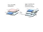
2 cases of antenna.jpg
Thank you very much. So FvM ! when I did the calculations explained above, I came up with lambda/4 length of 40mm ( assuming a FR4 substrate of PCB (ϵ=4.2) where I am mounting the antenna) So by going to 35mm of length i thought I wont be compromising on bandwidth .
But my basic confusion is still there. where should i place antenna if i provide a big ground plane??
Should I make 2 separate PCBs; 1 for antenna and its ground plane , and 2nd PCB for GSM module, provide a common ground to them and connect antenna to GSM Module via a shorting/jumping wire.
Or should I place them both in one multi-layer PCB but provide an exclusive Ground plane to antenna by dedicating one layer??? I am attaching the figures to explain my question. This is a rough sketch just to illustrate my question.
There is an added complexity to this problem. I have to house the GPS antenna later as well. :cry:
 

Unfortunately Er doesn't count for the ground plane effect in this case. The ground plane will almost act like a single metall sheet, no matter which PCB layer you use for it, E Kafeman already explained about the high coupling between layers.

The grond plane should extend over the full PCB area, unless the chip antenna specification demands a void. Having a copper pour (closely connected to the gound plane) on the chip antenna side might slightly reduce losses.

I think there's no problem to have both antennas on the same PCB side, provided GSM TX doesn't overload the GPS receiver.

I would perform antenna impedance measurements with the intended PCB shape as soon as possible, using state-of-the-art cable isolation techniques, to see if it achieves acceptable matching.
 
Thanks yes I am on designing test board for antenna.
GSM band being 900/1800MHz would then cause problem with GPS (1575 MHz) ??? By rough maths, I think that no second or third order harmonics fall in each others band.

So you are saying that GPS and GSM can coexist on one PCB but the GNP for an antenna should extend over the full PCB area. If i provide GSM antenna all of the GNP, then where should the GPS antenna go, Or should I connect same GNP to both antennas GND port?? But how would that work? My GSM module would be using GSM and GPS antenna simultaneously for location tracking and for sending SMS.
 
Last edited:

Status
Not open for further replies.

Part and Inventory Search

Welcome to EDABoard.com

Sponsor

Back
Top