Continue to Site

Welcome to EDAboard.com

Welcome to our site! EDAboard.com is an international Electronics Discussion Forum focused on EDA software, circuits, schematics, books, theory, papers, asic, pld, 8051, DSP, Network, RF, Analog Design, PCB, Service Manuals... and a whole lot more! To participate you need to register. Registration is free. Click here to register now.

Outline and ground plane for rectifier in Advanced Design System

Nathan1

Junior Member level 3
Joined
Jun 10, 2021
Messages
27
Helped
0
Reputation
0
Reaction score
0
Trophy points
1
Activity points
207
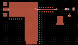
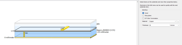
Hi, I am exporting a rectifier for fabrication. The Gerber file of my design does not contain a ground plane when exported. Does the ground layer need to be manually added to the layout based on my substrate setup? I think the design need a ground plane in this case especially when we have VIAs in the design.

How can I add an outline to this layout so that the fabrication company can easily determine the size of the rectifiers (length x width)?

Thanks a lot.
 

Attachments

  • Layout.png
    Layout.png
    21.7 KB · Views: 59
  • Substrate setup.png
    Substrate setup.png
    23.4 KB · Views: 56
Hi,

Some questions come to my mind:
* Why is the GND plane not included in the Gerbers at all?
* How did you export the Gerber files? (Commands)
* If you need focussed help you should tell what software you use.

Klaus
 
Hi,

Some questions come to my mind:
* Why is the GND plane not included in the Gerbers at all?
* How did you export the Gerber files? (Commands)
* If you need focussed help you should tell what software you use.

Klaus
Thanks, Klaus for your response. I am using Keysight Pathwave Advanced Design System software. I have attached a screenshot for exporting the Gerber file and the exported layers.
 

Attachments

  • 111.png
    111.png
    75 KB · Views: 61
  • exported layers.png
    exported layers.png
    37.8 KB · Views: 53
GND Plane is assumed as Present for ADS so you don't have to export Gerber file for GND, it's already default.
All you should do is to export Excellon Drill file for VIas. PCB Manufacturer will treat what rests.
You can send Gerber file for "cond" layer and drill file for "hole" layer.
 
GND Plane is assumed as Present for ADS so you don't have to export Gerber file for GND, it's already default.
All you should do is to export Excellon Drill file for VIas. PCB Manufacturer will treat what rests.
You can send Gerber file for "cond" layer and drill file for "hole" layer.
Thanks a lot, @BigBoss. Sorry, I'm not very clear here. Do you mean that the fabricated model will have a ground plane?

How to create an outline (length and width of the substrate) for this circuit and how much space should I keep between my design traces (on cond layer) and the edges of the outline? Is there any restriction?
If you order double layer PCB, it will have. Nowadays, almost all substrates have double layer.
You can use another arbitrary layer to define the "Outline" of the PCB. Draw your outline with a reasonable pitch-let say 0.5mm-1mm- then create another separate Gerber file for this additional layer then send it. You should explain the purposes of the layers to PCB manufacturer.
Outline layer will have a thick line as same as drilling tool diameter. If the board is a square, you can draw the corners only to indicate the drilling coordinates.
Thank you very much @BigBoss. @volker@muehlhaus Thank you, your comment is not visible here, but I can see it in myemail notification.
 
Hi, We provide the substrate thickness and permittivity value during the rectifier design in the advanced design system. The substrate's length and width are not specified. Do the length and width of the substrate affect the rectifier performance?

In my design, I have kept the edge of the substrate 1.5mm away from the rectifier design on cond layer (metal part).

Thanks a lot.

rectifier layout.png
 

LaTeX Commands Quick-Menu:

Part and Inventory Search

Welcome to EDABoard.com

Sponsor

Back
Top