Continue to Site

Welcome to EDAboard.com

Welcome to our site! EDAboard.com is an international Electronics Discussion Forum focused on EDA software, circuits, schematics, books, theory, papers, asic, pld, 8051, DSP, Network, RF, Analog Design, PCB, Service Manuals... and a whole lot more! To participate you need to register. Registration is free. Click here to register now.

GSM MIMO pcb antenna reposition

SWRmeter

Member level 1
Member level 1
Joined
Dec 24, 2019
Messages
34
Helped
5
Reputation
10
Reaction score
8
Trophy points
8
Activity points
173
I have these antenna modules for GPS and multiband GSM.
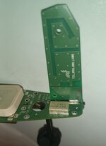
GSM GPS mimo antenna.jpegGSM GPS mimo antenna rev.jpeg

The vertical bit is for GSM, but I need to reposition it due to some mechanical constraints of my enclosure.

Q1: Would it be feasible to de-solder from the two feed-points, insert a short gap (about 5mm-10mm), and rewire the feedpoints ?
Q2: Is this likely to completely destroy the antenna characteristics, or maybe just degrade them, or have no effect at all ?
Q3: What would be the best way to do this to minimise any possible degradation ?

Thanks !
 
Last edited:

SWRmeter

Member level 1
Member level 1
Joined
Dec 24, 2019
Messages
34
Helped
5
Reputation
10
Reaction score
8
Trophy points
8
Activity points
173
Cross posting, since the high-tech guys in RF section don't seem to have basic answers.

I have these antenna modules for GPS and multiband GSM.
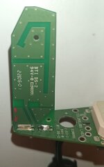
GSM GPS mimo antenna.jpeg GSM GPS mimo antenna rev.jpeg

The vertical bit is for GSM, but I need to reposition it due to some mechanical constraints of my enclosure.

Q1: Would it be feasible to de-solder from the two feed-points, insert a short gap (about 5mm-10mm), and rewire the feedpoints ?
Q2: Is this likely to completely destroy the antenna characteristics, or maybe just degrade them, or have no effect at all ?
Q3: What would be the best way to do this to minimise any possible degradation ?

Thanks !
 

vfone

Advanced Member level 6
Joined
Oct 10, 2001
Messages
5,538
Helped
1,598
Reputation
3,201
Reaction score
1,203
Trophy points
1,393
Activity points
35,184
Looks like the slanting feed line is just a 50 ohms transmission line, which (theoretically) its length has no much importance on in the radiation performance of the antenna.
Some problem would be with reducing the ground plane below the antenna (the bottom side triangles). Hopefully this could be no big issue because the antenna will use the ground from the horizontal PCB.
So I think will be no problem to introduce the gap that you want. At least a 5mm one.
 

SWRmeter

Member level 1
Member level 1
Joined
Dec 24, 2019
Messages
34
Helped
5
Reputation
10
Reaction score
8
Trophy points
8
Activity points
173
Looks like the slanting feed line is just a 50 ohms transmission line, which (theoretically) its length has no much importance on in the radiation performance of the antenna.
That is my thinking too. Though I was surprised when I calculated (using an online calculator - track width 1mm, gap width 1mm, FR4 board thickness 1mm) it came to ~73ohm, not 50ohm
Some problem would be with reducing the ground plane below the antenna (the bottom side triangles). Hopefully this could be no big issue because the antenna will use the ground from the horizontal PCB.
So I think will be no problem to introduce the gap that you want. At least a 5mm one.
My other concern is that -- Why is this particular length of transmission line even present ? Is it to make the entire antenna part at proper height above the lower PCB ground plane ?

The total height is ~5.5cm. The operational frequencies range from 700Mhz to 2700Mhz (GSM bands)
This height is exactly lambda/4 of the geometric mean of this freq range. So raising the whole bit by 5mm-10mm would possibly shift the effective band downwards .... IF this whole structure is supposed to be behaving like a monopole.

Or am I overthinking it ??
 

vfone

Advanced Member level 6
Joined
Oct 10, 2001
Messages
5,538
Helped
1,598
Reputation
3,201
Reaction score
1,203
Trophy points
1,393
Activity points
35,184
At the first sight looks like a Planar Inverted F Antenna (PIFA), but there is no ground connection to the radiating element.
I think it is a multi-band monopole antenna. The 75 ohms feddline impedance may be fine if this impedance match the antenna input impedance, and the impedance of the RX/TX stages.
A monopole antenna needs a ground plane. If the monopole is lifted from this ground plane will appear side lobes in the radiation pattern. For a cellular GSM antenna this may not be a big issue.
 

LaTeX Commands Quick-Menu:

Similar threads

Part and Inventory Search

Welcome to EDABoard.com

Sponsor

Top