Continue to Site

Welcome to EDAboard.com

Welcome to our site! EDAboard.com is an international Electronics Discussion Forum focused on EDA software, circuits, schematics, books, theory, papers, asic, pld, 8051, DSP, Network, RF, Analog Design, PCB, Service Manuals... and a whole lot more! To participate you need to register. Registration is free. Click here to register now.

gm of BJT and device size

Status
Not open for further replies.

mona123

Member level 5
Joined
Jun 10, 2010
Messages
87
Helped
3
Reputation
6
Reaction score
3
Trophy points
1,288
Activity points
1,898
gm of BJT is 40*Ic. So does it mean gm is independent of device size and shape? So I can get same gm with smaller device and larger device for same amount of current applied? Then why would one use large devices? Thanks.
 

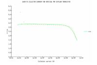
The device size is responsible for the range, where the gain (hFE) sustains an acceptable value, s. the foll. images for a lateral and a vertical integrated BJT:


High gain can only be achieved for a certain current density range. Larger currents need larger device sizes.

Different shapes are mostly found at discrete BJTs, in order to optimize RF and switching properties, as well as emitter efficiency.
 
gm of BJT is 40*Ic. So does it mean gm is independent of device size and shape? So I can get same gm with smaller device and larger device for same amount of current applied? Then why would one use large devices? Thanks.

I suppose, you know where the rough approximation gm=40*Ic comes from?
(gm=Ic/Vth with Vth=thermal voltage).
This formula describes the slope of the exponenetial relation between Ic and Vbe (Shockleys equation), which is valid for the ideal pn-junction only.
That means, it depends on temperature and may be applied for "small" currents Ic only (because for higher Ic values resistive and other effects come into play).
This relation does not depend on "device and shape" - however, the current gain and with it the input impedance does! And that's an important parameter.
 
So is gm a useless quantity in BJT then? Thanks.
 

Transconductance is seldom considered in a BJT it becomes more significant in FET amplifiers
 

Can you give some examples when gm is useful and when its not in a BJT? thanks.
 

So is gm a useless quantity in BJT then?
No it's a basic quantity in many design calculations. But other real word parameters need to considered additionally. You can find out yourself by reviewing design excercise problems in text books.
 

If it was clear in text book, i wouldn't have asked here:) If you know a particular section of a textbook that describes the importance of gm in BJT, that will be helpful. Thanks.
 

Trans conductance is not directly used in a BJT but in other forms in h parameter model design

the hoe and hie terms are more or less similar and collectively represent the Gm value of a tranny
 

If it was clear in text book, i wouldn't have asked here:) If you know a particular section of a textbook that describes the importance of gm in BJT, that will be helpful. Thanks.
I don't know about your text books. Mine are using gm in many places, e.g. Analysis and Design of Analog Integrated Circuits by Gray/Hurst/Lewis/Meyer. The role of the parameter gm corresponds to the description of the transistor as voltage controlled current source in basic transistor models. gm isn't but the derivative of Ic = f(Vbe).
 

Trans conductance is not directly used in a BJT but in other forms in h parameter model design

The opposite is true.
The transconductance gm=h21/h110(current gain/input resistance) is the most important parameter controlling the gain G of a BJT stage.
For example:

G=-gm*Rc (emitter stage without negative feedback)
G=-gm*Rc/(1+gm*Re) (emitter stage with Re-feedback).
 
  • Like
Reactions: FvM

    FvM

    Points: 2
    Helpful Answer Positive Rating
the model you are talking about is Z model and the one I meant was H representation of Tranny that is all the difference that is the reason why some of the books he referred are not having the ame in question

- - - Updated - - -

and do you mean hoe as trans conductance
 

the model you

who is "you"?
are talking about is Z model and the one I meant was H representation of Tranny that is all the difference that is the reason why some of the books he referred are not having the ame in question
- - - Updated - - -
and do you mean hoe as trans conductance

If you are referring to my last post - I didn't talk about any model, but instead about a physical parameter (slope of the Ic-vs-Vbe curve).
 

I meant mona 123 pal and I meant the books she referred has H models in detail and Z models dealt lesser
 

Gm is basically the gain however, Trans-conductance (Gm) is how well voltage (at gate or base) can be transferred into Current (drain or collector).
knowing Gm is just like having the gain if you want a certain output voltage but here you can control the output current.
 

Gm is transconductance which is the inverse of resistance and so it obviously clears you out pal
 

Yes Gm is the inverse of resistance

R = V/I
Gm = I/V, which is why i said it determines how well voltage can be transferred into current, i was not wrong in what i said
 

Yes Gm is the inverse of resistance

R = V/I
Gm = I/V, which is why i said it determines how well voltage can be transferred into current, i was not wrong in what i said

no one said you where wrong any where
 

I'm not happy with the explanation of resistance and transconductance as far as applied to transistor amplifiers.
R = V/I
Gm = I/V, which is why i said it determines how well voltage can be transferred into current, i was not wrong in what i said
I see several inaccuracies involved with the expression.
Unlike conductance as a general electrical quantity that can be calculated as G = I/V, transconductance of a transistor is a small signal parameter. This is expressed by the lower case letters in the formula sign. And it's not a ratio of static currents, it's a differential quotient respectively the slope of the exponential transistor characteristic, as explained in post #3.

Code:
Ic = f(Vbe)
gm = dIc/dVbe

Similarly, the input or output resistance of a transistor amplifier will be described as a small signal quantity and calculated as a differential quotient as well, e.g.
Code:
ro = dVce/dIc
 
  • Like
Reactions: LvW

    LvW

    Points: 2
    Helpful Answer Positive Rating
Status
Not open for further replies.

Similar threads

Part and Inventory Search

Welcome to EDABoard.com

Sponsor

Back
Top