Continue to Site
Follow along with the video below to see how to install our site as a web app on your home screen.
Note: This feature may not be available in some browsers.
Dear sir/madam, which simulation software did you use here? I guess the name is 'Simplis simulator'. I never heard of it before. Is it something equivalent to the P-spice? Thanks in advance.B does seem OK as Stewart states.
View attachment 185640
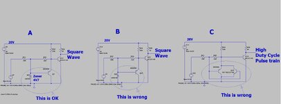
Circuit C does achieve very high duty cycle, based on delays between the coupled
NPN and PNP pair, but thats a very poor design due to device to device variation
and other T and V effects.
View attachment 185641
Regards, Dana.
Thanks thats exactly what i meant......A npn needs a diode placed with anode to base and cathode to collector....to sweep out charge carriers...in C, this diode is there, but is the wrong way round.....(its the diode in the PNP, ie the base-emitter diode).....so there will be storage time effects which will delay the switching of the BJTs.Circuit C does achieve very high duty cycle, based on delays between the coupled
NPN and PNP pair, but thats a very poor design due to device to device variation
and other T and V effects.