Continue to Site

Welcome to EDAboard.com

Welcome to our site! EDAboard.com is an international Electronics Discussion Forum focused on EDA software, circuits, schematics, books, theory, papers, asic, pld, 8051, DSP, Network, RF, Analog Design, PCB, Service Manuals... and a whole lot more! To participate you need to register. Registration is free. Click here to register now.

get me a softeare proper to make pcb with hole details too

Status
Not open for further replies.

rajaram04

Advanced Member level 3
Joined
Jun 17, 2012
Messages
871
Helped
6
Reputation
12
Reaction score
5
Trophy points
1,298
Location
earth
Activity points
7,687
hello sir
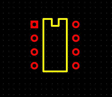
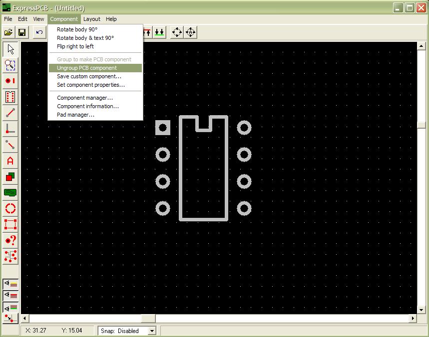
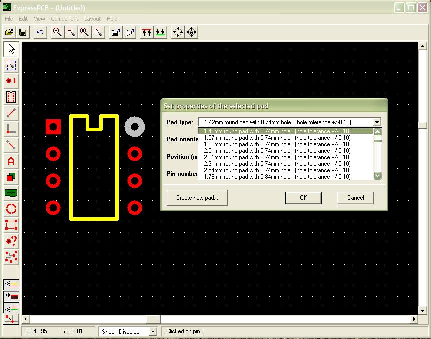
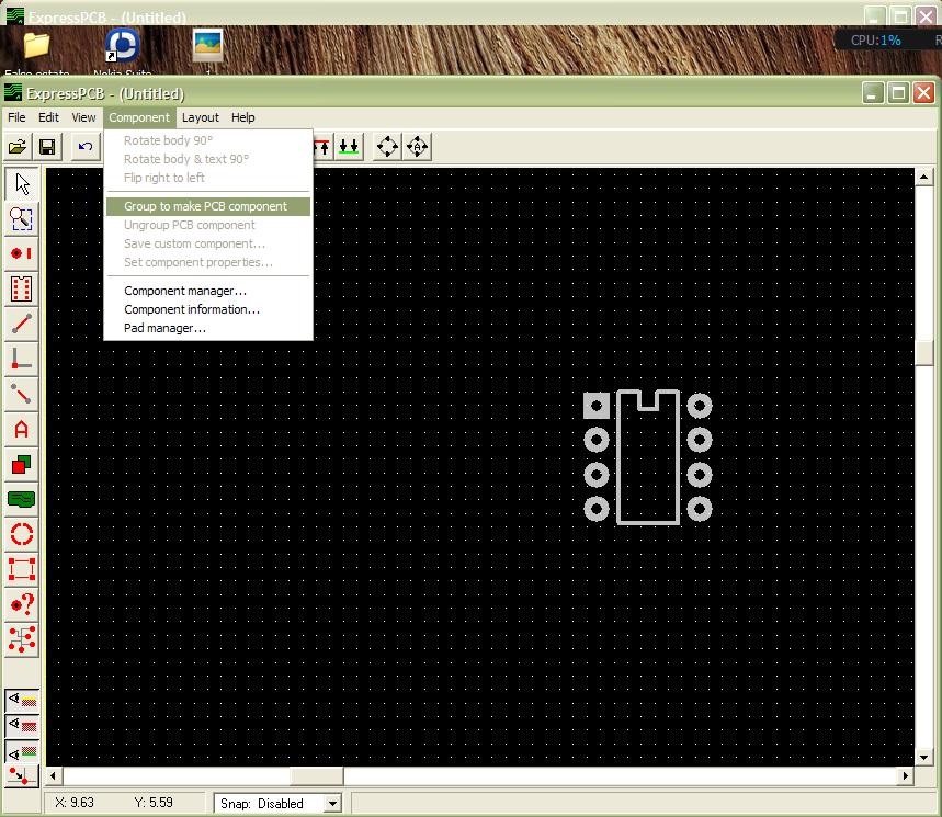
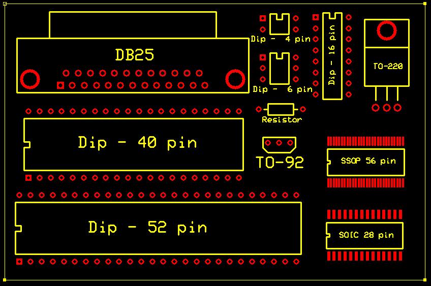
i want to make a clear desiging of my circuit on a pcb , so i want to make the design not only with copper platings connectors but with hole explanation there too , i designed in some softs but not able to mark holes there , actually i want to specify hole location so as to make ICs & other deligate components to be install properly in place with no stress , i jst want to make it like as we find them in market . Not much perfection clearity but needs connecting plates & holes simply , Too i ll make it with a simple chemical process further but please let me get a simple soft first
 

For me, the most simple software to make PCB designs is ExpressPCB. It is easy, flexible, simple & limited, and has basic component's footprints for your ease. So you no need to specify holes and pads all the time. You can make your own footprints and save them.
 

footprints bole to ? i mean here footprint means ?
 

Footprints means the original shape, size and positions of a component's pins. It is required to draw the PCB layout. They are already designed and saved in the software. Download and check it. You will understand. Here is an example....
 

ya ya boss what u told e3xactly its working & all going well , its awsome dear , thanks a lot lot lot :) are you an indian ?

- - - Updated - - -

ll pne more thing , if i want to make holes by penitrating via copper plates what would be the drill size ?
what precautions should be made regarding it ?
 

Yes, I am an Indian. I live in Kolkata.

The drill size is not an issue, as in India, probably all the PCB manufacturers uses manual drilling. So obviously they do not follow the drill size specification from your design. The will use same drill pin for every pad.
In ExpressPCB, all the DIP components have a very thin pad. You can't solder with that. So I recommend you to change the drill size according to your convenient. Follow the following tutorial...

1. First organize your components in the way you want. You can see the pad size is very small. Click on the component to select it.
6684617000_1363975361.jpg


2. In the menu bar, go to COMPONENTS> UNGROUP PCB COMPONENTS. Now all the elements of the component including the pads are edit-able.
7429273300_1363975362.jpg


3. Double click on each pad and select the desirable pad size. I would recommend pad size of 2.01mm or more. [DO NOT CHANGE THE ALIGNMENT OF THE PADS. THEY ARE POSITIONED BY JEDEC NORMS(2.54mm)]
3727554600_1363975363.jpg


4. When you are done editing, select all the elements of the component, go to COMPONENT> GROUP TO MAKE PCB COMPONENT.
7427833500_1363975364.jpg


This way you can make your own components and can save them.


Hopes this helps..
 

Yes, I am an Indian. I live in Kolkata.

The drill size is not an issue, as in India, probably all the PCB manufacturers uses manual drilling. So obviously they do not follow the drill size specification from your design. The will use same drill pin for every pad. %< %< %<

Looks that India is not a good place for outsourcing PCB's
 

Looks that India is not a good place for outsourcing PCB's

Yes. Definitely not if you want a high quality PCB. But yes, there are many organisations here who does these professional PCB jobs. From the above post, I meant for the ordinary local workshops. They are not so professional, but does our work....
 

Well, I make my own prototypes and all holes are drilled with the correct drill size as I would expect from even "not so professional" workshop.
My set of drills is as follows: 0.6; 0.7; 0.8; 0.9; 1.0; 1.1; 1.2; 1.3 and 3.175 mm (1/8").
From PCB shops, when producing doublesided boards, I'm expecting the holes to be as specified in PCB (Excellon - drill file), AFTER plating.
Single sided should also be drilled according to drill file.

A shop that drills holes with single drill would not earn for water, not to mention bread. :grin:
 

amazing genovator , speechless explanations here all in one go , i mean just best . . thanks a lot dear
so u r from india & from kolkata here ? gr8 , . . r u bengali or non ben. .

Zasto sir , its my pleasure to hv all your explanation here , actually i am doing a very non proffesional work & its first time for me to do like that , so face of the problem is a lil.bit diffrent here , thats why asking in details so that i coild make more easy arrangments over drilling & other issues . . i am thinking a lil.bit diffrent from what others do so planning for a new world . . ll tell you soon ;-)
 

For hobby project work, high quality PCB's are not needed. So I asked to neglect the drill size, since you are a hobbyist. But for professional work, you will get the exact PCB as per your design from your manufacturer. In ExpressPCB, design is simple, but there is only one catch... They do not provide any support to solder masking. Either you have to make the mask manually, or you have to give your design to ExpressPCB to manufacture. Right now, I am facing the same problem. Today I was supposed to give my design to my local manufacturer, but they said they need a masking file. :-?
 

hmm ya i came to know a few days ago here about it , now i am preparing a new system for it let c how much i ll get victory
 

Status
Not open for further replies.

Part and Inventory Search

Welcome to EDABoard.com

Sponsor

Back
Top