Continue to Site

Welcome to EDAboard.com

Welcome to our site! EDAboard.com is an international Electronics Discussion Forum focused on EDA software, circuits, schematics, books, theory, papers, asic, pld, 8051, DSP, Network, RF, Analog Design, PCB, Service Manuals... and a whole lot more! To participate you need to register. Registration is free. Click here to register now.

first pcb steps - sallen key filter

Status
Not open for further replies.
I haven't time to completely re-arrange things but maybe this will give you an idea.

Keith.
 

Attachments

  • TRY16.zip
    51.2 KB · Views: 40
THANK YOU VERY MUCH KATE !! It's extremely useful !! Just to know : running the Design Rule check appear some clearance errors due to the position of Vias. Are these problems negligible in your opinion ? Another question : what do you think about the idea to put other 13 opamp in this board (size : 10cm x 10 cm )?
 

You need to fix the DRC errors - I must admit I didn't check them as I was trying to show how you should arrange the components to minimise tracking.

Some of the design rules could probably be changed. Most places can handle 0.2mm tracks with no problem and 0.5mm drills. If you want to pack things in then use the smallest drill/pad you can for your manufacturer - that is where a lot of space disappears. You might want to use a finer grid than I used - I changed your grid to 1mm/0.5mm but maybe 0.25mm alternate grid would be better.

Ultimately, you want no DRC errors.

Do you mean another 13 opamps or 13 ICs?

Keith.
 
13 IC : total 15 ic + 2 connectors.

---------- Post added at 14:35 ---------- Previous post was at 14:35 ----------

how i decide tha size of wires ??
 

It would be a squeeze on that size board, but possible. I notice you are using 0402 components - have you tried soldering those yourself? I normally stick to 0603 unless something has severe size restraints. Putting components on both sides would help. This PCB is only 50x70mm and uses 0603.


For track sizes, I would normally look at 0.2mm to 0.3mm for analogue connections depending on track density and maybe 1mm where possible for power.

Keith
 
Prof. told me to use SMD components (0402 in this case), However next time I see him I am going to tell him your advice ! Meantime ,thank to you, I reach this result (see the attachment, thanks!): Have you any idea how to link power/ground to all 15 IC ?
30 signals from the first socket (the biggest one) should reach the IC, the other 30 should reach the second socket : have you an idea where to put these two socket in order to avoid tracks loops ? THX !!
 

Attachments

  • TRY17.zip
    53.2 KB · Views: 40

Normally you would pick a preferred direction for each side of the PCB. This doesn't have to be rigidly adhered to with an analogue board but some plan helps avoid getting trapped. So, you could run tracks vertically on the top, horizontally on the bottom or vice versa. You wouldn't rigidly stick to that otherwise you would end up with a huge number of vias. So, you could run the power vertically on the top layer between the IC legs. You would then run tracks horizontally from there on the bottom side to go to the connector.

Keith
 
ok! Last step !! Someone can give me and idea for tracking power and ground ? I don't have enough space ! Thank you !!!
 

Attachments

  • TRY18.zip
    53.7 KB · Views: 41

Your lack of a preferred direction for the top and bottom is why you are having trouble seeing a way through.

Keith.
 

Attachments

  • TRY19.zip
    54.2 KB · Views: 46

I'm not presently using Eagle and don't have a working installation on my computer, thus I'm unable to inspect the design files.

Generally, there should be at least at meshed ground net. Power supplies should preferably have bypass capacitors at each IC supply pin and don't need to be meshed. In my view, the filter topology is simple enough to have room for power supply and ground in a two layer design. A well considered placement is required, however.

As previously mentioned, 0403 seems unresonably small for the present application. You'll possibly face difficulties to get low T.C. capcitors (NP0 or similar dielectrica) in the intended capcitance range as required by a good filter. You would rather go for a smaller quad OP package (TSOP or chip scale package) to save board space.

Two sided component placement would allow ultimate circuit density, but doesn't make much sense without changing to a four layer PCB.
 
I added one more opamp in the schematic. Do you know why switching to the board it's not recognized ?
 

Attachments

  • try19.zip
    56.1 KB · Views: 38

Your schematic & board are not consistent. My guess is you added the extra opamp while the PCB was not also open. Once you have started a PCB, ALWAYS have it open when you have the schematic open.

Keith.
 
well, I deleted the third op-amp and re-added in the schematic with the board opened but nothing changed. Do you have any advice to resolve this problem ?
 

Hmm. I took your previous version, marked one block containing the opamp and all the connections in the schemtic, copied and pasted it. It appears on both the PCB and schematic. What exactly did you do?

Keith.
 

Attachments

  • TRY19kr.zip
    57 KB · Views: 43
did you try with the version of the 26-05-12, 09:33 post ?
 

That version has inconsistencies between the schematic and PCB. Once you have that problem you need to fix it so the schematic and PCB match before you can start to make modifications and expect them to be in sync. Go back to a version where the schematic and PCB are consistent and start from that. Don't use a version with consistency errors.

Keith.
 
yes Now it's all clear ! I noticed that you re-routed components !!! keith thank you very much !
 

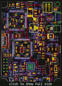
Tomorrow I have the meeting with Prof. to discuss about my progress. Someone could take a look to the job and maybe optimize it a little ? Moreover , does exist a command in Eagle that substitute all size of the wires ? Cause I think that 0,254 for my signals is too big (I should probably use 0,15). Thank you all !
 

Attachments

  • TRY21.zip
    58.7 KB · Views: 40

You can change wire sizes in bulk simply by selecting them all (group select) then changing the size. Turn off the view of everything else otherwise it may try to change the size of other things as well (e.g. text).

Keith.
 
in your opinion , is this pcb producible ?
 

Status
Not open for further replies.

Part and Inventory Search

Welcome to EDABoard.com

Sponsor

Back
Top