Tizana
Newbie level 6
Hi,
I'm currently designing my custom ARDUINO ZERO board with onboard sensors and lot others features. i looked in the internet for the schema of the ARDUINO ZERO and i found these two links :
schema 1 from adafruit: https://cdn-shop.adafruit.com/product-files/2843/Arduino-Zero-schematic.pdf
schema 2 : https://www.arduino.cc/en/uploads/Main/ArduinoZero-schematic.pdf
normally they are both identical but They have some differentiation (tiny one), i'll show it later.
the ARDUINO ZERO can be supplied by three differents power supply sources :
- From the External DC power supply (barrel jack) (12-7V)
- From the first USB1 which is connected to the onboard debugger IC
- From the second USB2 which is connected to the main microcontroller ‘SAMD21G18A’, this USB is an OTG usb which mean it can work as master or slave. and when it operate as master the arduino (‘SAMD21G18A’ microcontroller ) should provide the +5V power to the USB cable in order to feed the USB slave in the other side.
bellow is picture which resume little bit the power supply of the ARDUINO ZERO

In my actual design that i'm working on i will get rid of the Debugger which mean the USB1 will be removed. So my board will be feeded only by two sources , the external DC and the USB2 OTG.
Which mean in the schema 1 (page 3) the transistor Q200 and the two resistor R206 and R205 will be removed.
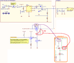
here's what it will look like my board power source :

as you can see in the screenshot it's a little bit messy because i had problem with my OTG power supply, and here's my questions :
1/the schema 1 & 2 of the original ARDUINO ZERO are not the same, in the schema 1 the resistor R207 (1M ohm) is between the GATE and the SOURCE of the Q201 while in the schema 2 the R207 is between the source and the 5V. which one is correct.
2/ i don't know if i have to put the resistor R208 which is between the SOURCE and DRAIN Q201. in the schema 1 they put a value 0 Ohm and in the schema 2 they put DNP (Do not populate)
3/ i need a to understand the USB OTG power supply circuit because it's little bit confusing.
For example, in case the USB OTG operate as a slave (ARDUINO side) normally the USB should be spplied by 5V from the USB, how can this USB 5v will feed the 3.3v regulator ? throught Q201? and in case both the external DC power and USB supplied at the same time the board we will have two sources in parallel which is wrong ?
and in case the USB OTG operate as a master so the board should provide the 5V to the USB. how did that happen ? through the Q201 transistor ? in this case the current will travel from the source to the drain ?
thx for taking your times to read this thread,
I'm currently designing my custom ARDUINO ZERO board with onboard sensors and lot others features. i looked in the internet for the schema of the ARDUINO ZERO and i found these two links :
schema 1 from adafruit: https://cdn-shop.adafruit.com/product-files/2843/Arduino-Zero-schematic.pdf
schema 2 : https://www.arduino.cc/en/uploads/Main/ArduinoZero-schematic.pdf
normally they are both identical but They have some differentiation (tiny one), i'll show it later.
the ARDUINO ZERO can be supplied by three differents power supply sources :
- From the External DC power supply (barrel jack) (12-7V)
- From the first USB1 which is connected to the onboard debugger IC
- From the second USB2 which is connected to the main microcontroller ‘SAMD21G18A’, this USB is an OTG usb which mean it can work as master or slave. and when it operate as master the arduino (‘SAMD21G18A’ microcontroller ) should provide the +5V power to the USB cable in order to feed the USB slave in the other side.
bellow is picture which resume little bit the power supply of the ARDUINO ZERO

In my actual design that i'm working on i will get rid of the Debugger which mean the USB1 will be removed. So my board will be feeded only by two sources , the external DC and the USB2 OTG.
Which mean in the schema 1 (page 3) the transistor Q200 and the two resistor R206 and R205 will be removed.
here's what it will look like my board power source :

as you can see in the screenshot it's a little bit messy because i had problem with my OTG power supply, and here's my questions :
1/the schema 1 & 2 of the original ARDUINO ZERO are not the same, in the schema 1 the resistor R207 (1M ohm) is between the GATE and the SOURCE of the Q201 while in the schema 2 the R207 is between the source and the 5V. which one is correct.
2/ i don't know if i have to put the resistor R208 which is between the SOURCE and DRAIN Q201. in the schema 1 they put a value 0 Ohm and in the schema 2 they put DNP (Do not populate)
3/ i need a to understand the USB OTG power supply circuit because it's little bit confusing.
For example, in case the USB OTG operate as a slave (ARDUINO side) normally the USB should be spplied by 5V from the USB, how can this USB 5v will feed the 3.3v regulator ? throught Q201? and in case both the external DC power and USB supplied at the same time the board we will have two sources in parallel which is wrong ?
and in case the USB OTG operate as a master so the board should provide the 5V to the USB. how did that happen ? through the Q201 transistor ? in this case the current will travel from the source to the drain ?
thx for taking your times to read this thread,