Continue to Site

Welcome to EDAboard.com

Welcome to our site! EDAboard.com is an international Electronics Discussion Forum focused on EDA software, circuits, schematics, books, theory, papers, asic, pld, 8051, DSP, Network, RF, Analog Design, PCB, Service Manuals... and a whole lot more! To participate you need to register. Registration is free. Click here to register now.

Discrepancy between experimental measurement and LTSpice noise simulation

Status
Not open for further replies.

frilance

Member level 1
Joined
Aug 16, 2012
Messages
37
Helped
0
Reputation
0
Reaction score
0
Trophy points
1,286
Activity points
1,703
Hi guys!

I wanted to compare the simulated noise in LTSpice with the experimental result measured using a Spectrum Analyzer (hp4395A) and I built the circuit you can see in the attached picture.
noiseSchem.PNG

The 50 Ohms load in the LTspice simulation represents the input impedance of the Spectrum Analyzer.

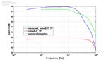
But as you can see in the Matlab plot of the output data, both results differ quite a lot (LTSpice in the order of 110 nV/sqrt(Hz) and around 60-70 nV/sqrt(Hz) in the Spectrum Analyzer)
noiseComp.png

I don't know what could cause this discrepancy. Are the spice models that bad? Am I doing something wrong in the simulation? The attenuation of the Spectrum Analyzer was set to 0 dB.

Thanks a lot in advance.

Cheers!
 

From the hand calculations the simulations shows good value of noise density (calculated are 127nV/sqrt(Hz)).
Check in your measurements dcOP of input BJT. Maybe your collector current is 4 times smaller caused smaller gm and finally two times smaller output noise.
 
I just checked, and it looks almost the same in both situations:

LTSpice Ic = (Vp-Vc) / Rc = (5 V - 0.796 V) / 3.9 K = 1.077 mA

Measured (Multimeter) dcOP Ic = (Vp-Vc) / Rc = (5.04 V - 0.862 V) / 3.9 K = 1.071 mA

I also checked all resistors values (to verify the non-inverting amplifier gain as well) and they are correct.

I did notice that discrepancy seems to have a factor of 2 in it... and it looks quite suspicious.

Dzięki!
 

Now I noticed voltage divider at the output. Are You sure that You are looking for noise density at the out node? Taking into account the voltage divider gives 64nV/sqrt(Hz) of noise density confirmed by measurements.
 
That's what I meant at the beginning with

"The 50 Ohms load in the LTspice simulation represents the input impedance of the Spectrum Analyzer."

So in the implemented circuit, the 50 Ohms of load are not there, and I measure the output voltage noise density being this voltage the one over the SA 50 Ohms input. Isn't that the same thing I'm doing in LTSpice by placing the 'out' node where I did?

According to that, both results should represent the same thing, taking into account the voltage divider already.
 

I don't know LTSpice tool so I asked this stupid question ;-)

The only thing which came to my mind is to check if the input BJT has proper transconductance value (around 42mS).
 
You would identify the dominant noise sources in the simulation and check against the transistor specification. An inaccurate transistor model could well explain the differences.
 
Actually I tried it yesterday, by plugging in the output of a Network Analyzer into the bjt's base (as in the LTSpice schematic) and measured the transfer function in the frequency range. And it was 5.5 dB higher than in LTSpice (41.5 dB vs 47 dB)....

First, I don't understand this discrepancy either since the bias conditions are the same (and the OpAmp gain) and second, with a higher gain I would expect a higher output noise, not lower ???

- - - Updated - - -

I attach the plot with both TFs. The difference it's slightly bigger, closer to 6 dB.
 

Attachments

  • comparisonTFs.png
    comparisonTFs.png
    58.3 KB · Views: 83

Since your actual circuit has a cutoff frequency of only 40MHz but the Spice circuit has 100Mz then I think you built your circuit on a solderless breadboard with many connecting wires all over the place and lots of stray capacitance between the wires and all the rows of contacts. The increased gain from your circuit might be caused by poor connections in the contacts and/or positive feedback from the stray capacitances.
 
It's a double sided PCB, with mainly MINIMELF Resistors and other SMD components...
 

Well, I run a simulation with Genesys and a more accurate model of the transistor (S-parameters for Ic= 1 mA and Vce = 1.5V - I have Vce= 1.636V)... and look. It seems that the LTSpice's model is waaaay off.

I could not find any other model for my BFR181 than this BFR181/SIE... but anyway, seeing this, I think I can't trust LTSpice that much.

Btw, the response from 1MHz to 10MHz for the BFR181 in Genesys was extrapolated, since the model does not have values in that frequency range.
 

Attachments

  • comparisonTFsWgenesys.png
    comparisonTFsWgenesys.png
    49.6 KB · Views: 119

Status
Not open for further replies.

Part and Inventory Search

Welcome to EDABoard.com

Sponsor

Back
Top