Continue to Site

Welcome to EDAboard.com

Welcome to our site! EDAboard.com is an international Electronics Discussion Forum focused on EDA software, circuits, schematics, books, theory, papers, asic, pld, 8051, DSP, Network, RF, Analog Design, PCB, Service Manuals... and a whole lot more! To participate you need to register. Registration is free. Click here to register now.

Diodes in parallel PCB Layout

Status
Not open for further replies.

neonwarrior

Member level 2
Joined
Dec 23, 2010
Messages
47
Helped
4
Reputation
8
Reaction score
4
Trophy points
1,288
Activity points
1,610
Hello everyone I wonder which PCB layout is best to parallel diodes.
Please see attached image.
Diodes in parallel pcb layout.png

There are two figures from application note AN599 from ST. (Good and bad layout B & A)
And the third one is another possible layout that I saw on a Welder (Actually with 3 TO-247 diodes in parallel).
Thanks in advance
 

Take the case of more than two diodes. "B" scales with more than two. Just keep making the "in" and "out" connections at the opposite ends. "A" gets worse. Now, where do you put the in and out on the Welder layout and still be balanced? I agree that with two it looks pretty good.
 
B equalizes resistance seen by each diode so they will carry like currents assuming they are matched for forward voltage. C will result in higher resistance as you move out from the central connection. The diodes further away from the center will carry less current due to the larger resistance seen by the current.
 
Thanks for your replays
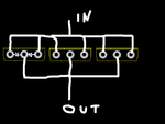
Hey Analog ground the three (diodes x 2) are connected like this image

Three TO 247 diodes.png

It seems that it is not so good...
 

Well, not as balanced. This all depends on the speed of the signals you are switching and the length and width of traces. Very fast signals are going to be more unbalanced then very slow signals, and very large currents are going to be more unbalanced than very small currents. In your drawing the middle diode pair will conduct more current assuming the Vforward of the diodes are matched. If you are switching signals that transition in the less than 100 nsec then the inductive effect of the traces will cause the unbalance to worsen. The faster the signals, the more unbalance.
 
Status
Not open for further replies.

Similar threads

Part and Inventory Search

Welcome to EDABoard.com

Sponsor

Back
Top