imrankhanPNU
Member level 1
Hello everyone,
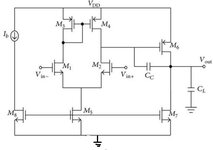
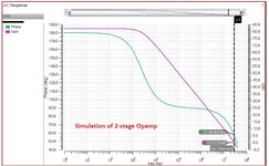
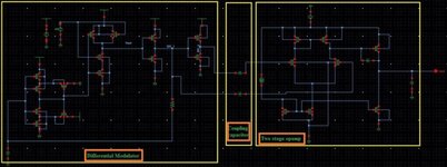
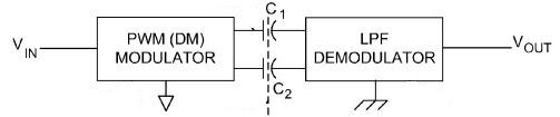
I am designing LPF based differential demodulator(LPF_DDM) to retrieve differentially modulated signals, which are on-chip capacitive isolated [shown]. LPF_DDM includes a differential amplifier, LPF, and Schmitt trigger. I designed a two-stage opamp [specification below], as a differential amplifier. Simulation results of the 2-stage opamp matched with desired specifications (GBW, Phase margin, gain, etc ). However when the differential modulated signals are given as input, then opamp does not work.
Is my 2-stage opamp design and/or design parameters adequate for differential modulated input signal?
Thanks.
Design Parameters:
Input common mode range: ICMRmax = 4V; ICMRmin = 1.5V ; Load capacitance =2pF ; Gain = 1000/60db ; Slew-rate (SR) = 20v/usec. GBW=30MHz
Phase margin (PM)>= 60-degree