Continue to Site

Welcome to EDAboard.com

Welcome to our site! EDAboard.com is an international Electronics Discussion Forum focused on EDA software, circuits, schematics, books, theory, papers, asic, pld, 8051, DSP, Network, RF, Analog Design, PCB, Service Manuals... and a whole lot more! To participate you need to register. Registration is free. Click here to register now.

Differential amplifier scaled to operate with -230 volts AC to feed a microcontroller works as expected in LTspice simulation. However, the gain is no

thannara123

Advanced Member level 5
Joined
Jan 7, 2010
Messages
1,580
Helped
122
Reputation
244
Reaction score
114
Trophy points
1,353
Location
India
Activity points
10,384
Hi experts ,
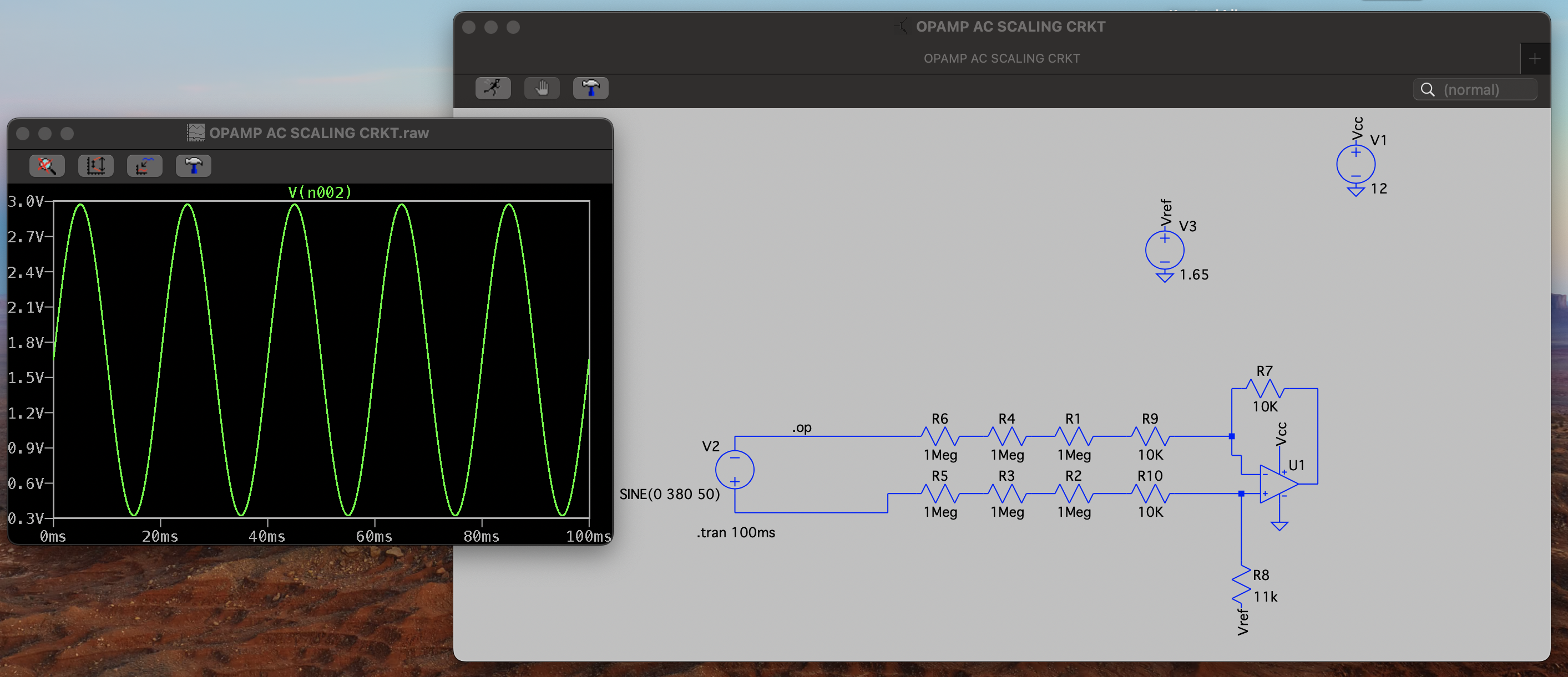
see the image
Screenshot 2024-04-18 at 8.19.00 PM.png


0 to 260 volts AC at 50 Hz is supplied to a resistor network, as shown in the circuit above. The op-amp and series resistor are used to scale down the voltage for sensing by a microcontroller.. An offset dc voltage 1.65 volt is given to the inverting input to shift the ac wave as required .
In the above simulation the circuit and its output is worked as expect .

However, in the real world, my circuit does not perform as expected. The gain is not matching the calculated values; instead, it is higher. Changing the feedback resistor does not yield the expected effects according to the calculations. Look the video the signal is distroying when icreas the input ac volt


Any help is appreciated.
--- Updated ---

using op amp is LM358 ,
 
Last edited:
1) Is your input TRULY floating, as it is in your simulation?
2) It's impossible to see what the scale is on your scope. There's way too much garbage on the screen.
3) You say the gain is off, but don't give any information. Is it off by a factor of 10000000000000?
4) Same for "Changing the feedback resistor does not yield the expected effects...". What ARE your expected effects? We're not mind readers, you know.
 
Hi,

in addition to Barry´s post...
* R8 should have the same value of R7 ... other wise you get bad CMRR.
* you need to test your simulation for both extremes of input range: Do a test with the lower end of V2 connected with GND. And also the upper end.
* the power supplies need bypass capacitors.
* you should limit the bandwidth to focus on the frequency range of interest

***
I recommend to replace R8 with two resistors of twice the R8 value: One connected to GND, the other connected to 3.3V (In case you use an ADC: connect to ADC_VRef)

I usually avoid to power the OPAMP from 12V , I rather use %V or 3.3V .. what already is available. This also avoids the need for a voltage limiter.

Btw: the video is unavailable for me. (But I avoid to watch videos anyways)

Klaus
 
Waveform shows that input common mode range is exceeded, even causing phase reversal. It looks actual supply voltage is not 12V.

I agree with the assumption that simulation mismatch is caused by floating voltage source. In real circuit, we probably have a grounded voltage source, increasing common mode voltage if negative terminal grounded.
 
In the real world - we cannot see the relationship between the centre point of the 230Vac and the centre point of the +/- 12 ~ 18V supplies you should be using

The relationship of these is a major factor in whether this circuit will work well or not.

In any event - this ckt could be designed way better to get the signal out you require
 
Changed the R8 with same as R7 . Power supply changed to 3.3v ,Added a filter capacitor . in real circuit a i already added power supply capacitor .

@ KlausST
** you need to test your simulation for both extremes of input range: Do a test with the lower end of V2 connected with GND. And also the upper end.

sir i checked both levels at low level it shows with expected gain . but at higher level above 70 volt it destroys the waves .


If R7 is 10kil ohm , serial resistor values Total resistor 3.01meg
so the gain is 0.00332278

if Vpeak is 380 (rms 268volt) the gain would be
380*0.00332278 = 1.26
The offset volt (dc to shift). is 1.65volt
so the output maximum peak volt would be 1.26+1.65 =2.91
In simulation it is correct
But in real circuit Vpeak is 3.2 volt is getting ,but expected 2.91. (it is just for sample desgin .i will do actual desgin after after correcting the circuit)

I am attaching some image at each voltage of input to better understand the issue


@ 90RMS (Vpeak 127) volt Input the output of diffrential amp shows below
WhatsApp Image 2024-04-19 at 7.34.29 AM.jpeg


@ 125RMS volt Input the output of diffrential amp shows below
WhatsApp Image 2024-04-19 at 7.34.28 AM.jpeg


@ 171RMS volt Input the output of diffrential amp shows below
WhatsApp Image 2024-04-19 at 7.34.28 AM (1).jpeg


At @171 the wave is completely destroyed , But if i Increase the dc level offset volt ie to shift the signal 1.65 to a higher level the wave canot be destroy .

whats the wrong with I am please help me .

If any information require i am ready to give sorry for my bad english and explanation .
--- Updated ---

The following is my Testing circuits
WhatsApp Image 2024-04-19 at 7.44.58 AM (1).jpeg
WhatsApp Image 2024-04-19 at 7.44.58 AM.jpeg
 
@ KlausST sir :I recommend to replace R8 with two resistors of twice the R8 value: One connected to GND, the other connected to 3.3V

I wil do and post the result thankyou .
--- Updated ---

sir what is the necessity of this type spliting circuit ?
 
Last edited:
Why don't you show the real circuit, including voltage regulator and trimmers. Most likely the problem is that "Vref" is no voltage source but a voltage divider with output impedance adding to R8.
 
Why don't you show the real circuit, including voltage regulator and trimmers. Most likely the problem is that "Vref" is no voltage source but a voltage divider with output impedance adding to R8.

sorry sir circuit will be post soon

So I need a buffer to give a constant voltage refferance volt ?
in web i have seen ,most of using opamp based buffer.
 
Hi,

as far as I see your calculations are correct.
You only calculated the expected output, but you missed to caclulate the voltages at the OPAMP inputs.
Indeed you just need to calculate the voltage at IN* (because IN- will regulate to the same voltage)

The voltage at IN* is: V_IN+ = 1.65V + (V_P -1.65V) * 10k / (3010k + 10k)
1) when V2 lower input = GND; V_P = 0V: V_IN+ = 1.65V + (0V -1.65V) * 10k / (3010k + 10k) = 1.644V
2) minimum when V2 upper input = GND; V_P = -380V: V_IN+ = 0.386V
3) maximum when V2 upper input = GND; V_P = +380V: V_IN+ = 2.903V

Now compare this with the CommonModeInputvoltageRage of your OPAMP (CMIR). TI LM358 datasheet says: V_ ... to V+-2V, so 0V ... VCC
1) is uncritical.
2) is inside VCIM
3) is outside if you use 3.3V. It is inside as long as your supply voltage is more than 4.9V.

So my recommendation to use 3.3V does not work for the LM358. (Sorry for this. I don´t use LM358) LM358 is no "RAIL-TO-RAIL_INPUT" OPAMP.
--> It shold work with LM358 and supply of 5V
--> or with an RR-Input OPAMP and 3.3V supply
****

As FvM stated .. there may be something wrong with your power supply. Please verify stable supply voltage, especially when you see erroneous output.

***

Also we don´t see where your 1.65V come from. It is important to be stable and low impedance.
This 1.65V are important for proper opration, tus you should include it in the schematic you show us.

--> When you use a resistive divider then it causes a "source resistance". This means the 1.65V will move when current is drawn from this 1.65V source.
--> Verify stable 1.65, especially when errors happen.

Now to my recommendation to use two resistors instead of R8. (It was a recommendation, not a MUST)
If you use 20k to GND and 20k to 3.3V, then this equals a 1.65V voltage source with a series (also called SOURCE) resistance of 10k Ohms. Exactly what you want.

We don´t know what you do with the OPAMP output. Please tell us.
In my case I often wire the OPAMP output to an ADC. In this case it´s the most precise and most simple solution to use 20k_to_GND and 20k_to_ADC_VRef.

****

I see you have this circuit twice, because there are two OPAMPs in one package.
--> Verify that the second (unused) OPAMP output is not saturated. I have had OPAMPs that got confused when their second OPAMP got into saturation.

Klaus
 

LaTeX Commands Quick-Menu:

Part and Inventory Search

Welcome to EDABoard.com

Sponsor

Back
Top