Continue to Site

Welcome to EDAboard.com

Welcome to our site! EDAboard.com is an international Electronics Discussion Forum focused on EDA software, circuits, schematics, books, theory, papers, asic, pld, 8051, DSP, Network, RF, Analog Design, PCB, Service Manuals... and a whole lot more! To participate you need to register. Registration is free. Click here to register now.

decoupling capacitors for improving pulse signal on the laod

yefj

Advanced Member level 4
Joined
Sep 12, 2019
Messages
1,195
Helped
1
Reputation
2
Reaction score
3
Trophy points
38
Activity points
7,217
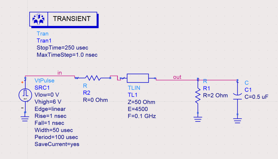
Hello,I am trying to simulate the effect of improving a square pulse with decoupling capacitors.
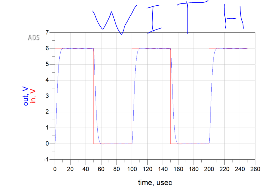
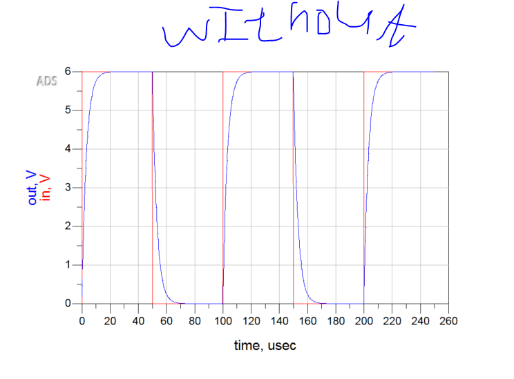
One plot i with 0.5uF on the load and the other is without .The capacitor didn't help much with improving the pulse on the load to be as close as possible to the input one.
i know that the result on the load is a sum of reflected waves going back and forth.
is there a way based on transmission line reflection theory to know what decoupling capacitors should i use to deliver a signal as close as it was at the input?
Thanks.
1701092508666.png

1701091864478.png


1701091845164.png

1701091937908.png
 
Your question does not resemble a matched load for pulse transmission. Actually the parallel load cap resembles a short circuit temporarily and open circuit to DC. All wires have inductance including ground wires so if used for CMOS which are like switches with capacitance, when many switches occur in parallel inside an IC with x pF per gate this switched resistance draws current from the inductive wires which will inject a negative transient voltage. Adding a decoupling cap say 100x bigger than all the switched capacitance in each chip directly across Vdd:Vss reduces that current pulse from spreading to other IC's and thus decouples the current pulse from DC & GND bus

In this scene the cap is across the DC bus load to decouple spikes to and from the DC transmission line which is not what you have described but maybe intended. Please verify or explain better what you are simulating.
 
Hello Stewart, I assume my IC is 2 Ohm resistor.
my input source is a pulse from 0 to 6.
The transmission line is just a way to simulate how a pulse can be distorted.
I want to see a case where decoupling capacitors improve a distorted signal.
could you please recommend me such situation ,so i could see it work?
Thanks.
 
That is insufficient info to define a model of a power supply, load and signal source and has no resemblance to your fig. 1. A decoupling cap lowers AC impedance and will not match source or load to your transmission line.
 
Hello Tony ,my goal to simulate the effect of a decoupling capacitors.
Could you please recommend me some PULSE input structure so i could see how they fix distorted signal?
Thanks.
 
Hi,

When I read "decoupling capacitors for improving pulse signal"..
I think about a decoupling capacitor in parallel to the power supply at the driver side.

But you put the capacitor at the load side. I can´t imagine how this could improve the signal at all.
It always causes high current at every signal edge. Slowing the edge down. So: ... no improvement.

***
Please tell us where this idea is from: Link to a document.

Klaus
 
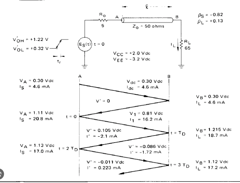
Hello Klaus,from the eric bogatin booul there is a system i tried to resemble as shown below in my ADS simulation.
I am looking for a simple case where a decoupling capacitors fix distorted pulse signal so i could investigate it.
Thanks.

1701106098701.png


1701106334700.png
 
Step 1. Analyze , or model the problem (logic diagram) before asking for a solution

Not simply a box with PDN
Assume all conductors have inductance and all dielectrics have ESR & ESL and all sources may have Rs L and all R loads have C and L and all switch CMOS also switches capacitance current from Vdd during transition. Also all 10:1 probes have ESL on ground leads, Any or all of this produces unwanted ringing from resonant transfer function.

Al trasces, wires and cables have a "Characteristic Impedance" and delay per unit length

So spectrum and or rise time is affected. A scope timing diagram could but does not explain this.

Which risetime and problem are you wanting to simulate and fix?
 
Last edited:
Comparing post #1 and post #7, I wonder which problem is modeled at all?
Post #1: pulsed voltage source with constant load
Post #7: constant voltage source with pulsed load
Please clarify.
 
Hello Klaus, sorry for the missunderstanding.As you can see the book photo and the photo on post 1.
I have marked in red arrows how i tried to simulate the system in the book.
i want to see a "bad " situation and then how it gets better by adding a decoupling capacitors.

1701110039466.png


1701109937972.png
 
Hello Klaus, sorry for the missunderstanding.As you can see the book photo and the photo on post 1.
I have marked in red arrows how i tried to simulate the system in the book.
I don´t have the book, nor a link to it.
I don´t know which photo exactly.
So I can only guess you refer to the test first circuit with voltages and timings ... then I miss the context.

Klaus
 
Before looking at the requirements for a PDN, examine a CMOS logic signal on a long wire with 10:1 probe and very short ground clip. <2cm using some unknown load capacitance. The CMOS will have some source resistance Vol/Iol= Rs typically 25 Ohms say +/-30% for 5.5V logic family .

A 1 MHz square wave might look something like this. Now we know delay lines, cables with some Zo can be represented by a lumped Zo and fo resonance with a Q ratio of reactive/real resistance or I^2R = power ratio.

The schematic is just logical and not analog so it assumes you know about RLC parasitics. You might consider the tradeoffs of trying to match the source or load or both on ringing and loading attenuation of 50% from matched sources and loads typical for RF.

1701110318005.png


This simulation is interactive with a dummy logic diagram on top and some real model of CMOS driving a wire with "ideal' switches and wires connecting the logical passive parts that are somewhat realistic values for physical setups with a long wire to say a breadboard and ideal scope probing with an inductive ground clip.

Next try switching a load resistor on or off. Notice ringing is reduced when somewhat matched and there is also attenuation,

Now open switch and open the switch across the source R to raise the source impedance.

Note that the Zo of √ L/C ratio has a value and choosing a source or load near this value attenuates the reflections that cause ringing at one end or the other.

Now which one is preferable for CMOS logic ? Well that may depend if the signal is prone to CM noise, then you want it differential and matched at both ends and allow 50% loss.


My Falstad Simulation above.

Now how can one model a PDN (pulse delivery network)? What is it's purpose?
? Provide DC over the spectral density and power range {V,I, Z) with the lowest acceptable AC noise.

This commands an expert knowledge of low ESR caps, low Rs source for load regulation Effective series inductance (ESL) of all conductors and ESL, ESR of all dielectrics or loss tangent of the dielectric.

It might look completely different than a 100A 600V EV load but still it must be modelled to determine the optimal PDN.

Inductors and transformers are rarely effective more than a couple frequency decades and capacitors tradeoff high C with high ESR and high ESL so an array of C values are needed to spread the low spectral impedance and prevent unwanted resonances.

This might be a more complex electromagnetic-physical problem until you understand the properties of transmission lines, striplines and microstrips and how to model the load and delivery complex impedance so as to design the ideal source near the load. Some of this is taught in EMC 101 but is described well in Eric Bogatin's Signal Integrity book or to some extent in Henry Ott's EMC book in www.archive.org.

Also search YT for similar


--- Updated ---

Before looking at the requirements for a PDN, examine a CMOS logic signal on a long wire with 10:1 probe and very short ground clip. <2cm using some unknown load capacitance. The CMOS will have some source resistance Vol/Iol= Rs typically 25 Ohms say +/-30% for 5.5V logic family .

A 1 MHz square wave might look something like this. Now we know delay lines, cables with some Zo can be represented by a lumped Zo and fo resonance with a Q ratio of reactive/real resistance or I^2R = power ratio.

The schematic is just logical and not analog so it assumes you know about RLC parasitics. You might consider the tradeoffs of trying to match the source or load or both on ringing and loading attenuation of 50% from matched sources and loads typical for RF.

1701110318005.png


This simulation is interactive with a dummy logic diagram on top and some real model of CMOS driving a wire with "ideal' switches and wires connecting the logical passive parts that are somewhat realistic values for physical setups with a long wire to say a breadboard and ideal scope probing with an inductive ground clip.

Next try switching a load resistor on the off. Notice ringing is reduced and there is also attenuation,
Now open switch and open the switch across the source R.
Note that the Zo of √ L/C ratio has a value and choosing a source or load near this value attenuates the reflections that cause ringing at one end or the other.

Now which one is preferable for CMOS logic ? Well that may depend if the signal is prone to CM noise, then you want it differential and matched at both ends and allow 50% loss.


My Falstad Simulation above.

Now how can one model a PDN (pulse delivery network)? What is it's purpose?
? Provide DC over the spectral density and power range {V,I, Z).

This commands an expert knowledge of low ESR caps, low Rs source for load regulation Effective series inductance (ESL) of all conductors and ESL, ESR of all dielectrics or loss tangent of the dielectric.

It might look completely different than a 100A 600V EV load but still it must be modelled to determine the optimal PDN.

Inductors and transformers are rarely effective more than a couple frequency decades and capacitors tradeoff high C with high ESR and high ESL so an array of C values are needed to spread the low spectral impedance and prevent unwanted resonances.

This might be a more complex electromagnetic-physical problem until you understand the properties of transmission lines, striplines and microstrips and how to model the load and delivery complex impedance so as to design the ideal source near the load. Some of this is taught in EMC 101 but is also described well in Henry Ott EMC books in archive.org and
--- Updated ---

Understanding how to have test points, take measurements, understand them then improving the results is what LeCroy CTO calls, getting it right the 2nd time. The benefits of learning to be a Test Engineer while doing design with the understanding of all the RLC properties of materials. After all these are only 3 variables.
 
Last edited:

LaTeX Commands Quick-Menu:

Part and Inventory Search

Welcome to EDABoard.com

Sponsor

Back
Top